X-Ray Diffraction on Vertically Modulated Superlattices
P. Machovec, L. Horák
Charles University in Prague, Faculty of Mathematica and Physics, Czech Republic
petr.machovec@mff.cuni.cz
Superlattices are widely investigated for their unique electronic and magnetic properties. Recent advances in deposition methods have allowed the creation of much more complex superlattices with promising applications such as solar cells, sensors, spintronics, and data storage. This requires very precise tuning of the deposition process. One of the challenges of creating high-quality superlattices is the precise control of the amount of deposited material. In our work, we present a new method for post-deposition calibration of the deposition process.
If the amount of material deposited for each layer is more or less than the exact amount needed for one layer, the resulting superlattice has vertical modulation. This means that the chemical composition of the superlattice has a period that is not equal to an integer number of monolayers. We can characterise this by a parameter Λ called wavelength of modulation, which is the vertical period of chemical composition. Figure 1 shows the difference between ideal and modulated superlattice.
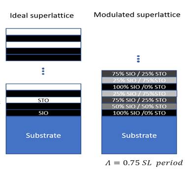
Figure 1. Schematically shown the difference between the ideal (left) and modulated (right) superlattice. The ideal superlattice is 2(SrIrO3)/1(SrTiO3)/1(SrIrO3)/1(SrTiO3). The modulation wavelength of the shown superlattice is 0.75 of the ideal superlattice period.
The x-ray diffraction on the modulated superlattice is calculated by the following process. First, the occupancies of each material for each layer are calculated from the wavelength of modulation. And then, the structure factor of the superlattice is calculated by the following formula:
|
|
(1) |
where ![]() is the fraction of
sites occupied by material 1 in the j-th layer,
is the fraction of
sites occupied by material 1 in the j-th layer, ![]() is the vertical
position of the j-th layer calculated by Vegard's law and
is the vertical
position of the j-th layer calculated by Vegard's law and ![]() and
and ![]() are the structure
factors of materials 1 and 2.
are the structure
factors of materials 1 and 2.
Vertical modulation causes a systematic shift and splitting of superlattice maxima in 2Theta/Theta scans. Additionally, it is possible to include lateral inhomogeneity of the layers into the simulation. This causes a broadening of the superlattice maxima. In Figure 2 we show simulation and measurement of 2Theta/Theta scan of 2(SrIrO3)/1(SrTiO3)/1(SrIrO3)/1(SrTiO3) superlattice with the vertical modulation period equal to 0.975 of the ideal superlattice period.
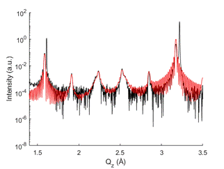
Figure 2. 2Theta/Theta scan of 2(SrIrO3)/1(SrTiO3)/1(SrIrO3)/1(SrTiO3) superlattice with modulation 0.975 of superlattice period. Measured data are plotted in black and simulation in red.