Structure and microstructure in (111) and (111)+(001) ScN/MgO thin films
E. de Prado, J. More Chevalier, S. Cichoň, L. Fekete. J. Lančok
Institute of Physics of the Czech Academy of Sciences, Na Slovance 2, 18221 Praha 8, Czechia
prado@fzu.cz
ScN is an emerging semiconductor that exhibits rock-salt (cubic) crystalline structure [1]. It is of high interest in material science due to its physical properties such as high melting point and high electron mobility. To improve the mobility and other electronic properties, it is necessary to produce single crystal ScN thin films with low density of defects. It has been demonstrated that the presence of point defects and impurities affects thermoelectric properties [2]. Planar defects such as twins have been also explored for (111) and (001) ScN thin films grown on different substrates [1], [3]–[5]. The presence of twins for bi-oriented (111)+(001) ScN films on MgO (001) has been reported [6] but its origin is not fully understood yet. In this work we pay special attention to the system (111)+(001) ScN/MgO (001) and we compare our results with single oriented (111) ScN films. To it, several ScN films were deposited on MgO (001) substrate by DC reactive magnetron sputtering at different temperatures. The morphology of the films has been explored by Atomic Force Microscopy (AFM) and the presence of twins has been analyzed by X-Ray Diffraction through 2theta scans, and 002, 022, and 111 pole figures.
|
|
|
|
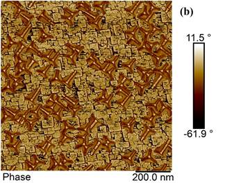
Figure 1. Results for bi-oriented ScN films. (a) 002 Pole figure and (b) AFM image with phase contrast. |
|
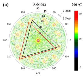
For the bi-oriented kind of films a very complex system of twins is obtained (Figure 1), which can be separated in the contribution of two, one coming from the (001) ScN oriented crystals and the other one coming from the (111) crystals. A deep study of the structure and microstructure of such a system could provide a better understanding of the role of twins in the final film orientation.
Keywords: ScN; twins; pole figure; epitaxial layer
[1] M. A. Moram, T. B. Joyce, P. R. Chalker, Z. H. Barber, and C. J. Humphreys, “Microstructure of epitaxial scandium nitride films grown on silicon,” Appl. Surf. Sci., vol. 252, pp. 8385–8387, 2006.
[2] S. Kerdsongpanya, B. Alling, and P. Eklund, “Effect of point defects on the electronic density of states of ScN studied by first-principles calculations and implications for thermoelectric properties,” Phys. Rev. B - Condens. Matter Mater. Phys., vol. 86, no. 19, pp. 1–7, 2012.
[3] S. Acharya et al., “Twinned growth of ScN thin films on lattice-matched GaN substrates,” Mater. Res. Bull., vol. 143, no. January, p. 111443, 2021.
[4] E. de Prado, J. More-Chevalier, S. Cichoň, and J. Lančok, “Twin domains of ScN (001) films on MgO (001),” Acta Crystallogr. Sect. A Found. Adv., vol. 77, no. a2, pp. C835–C835, 2021.
[5] S. Chowdhury et al., “Synthesis and study of ScN thin films,” pp. 1–13, 2021.
[6] J. More-chevalier et al., “Applied Surface Science Correlation between crystallization and oxidation process of ScN films exposed to air,” Appl. Surf. Sci., vol. 515, no. December 2019, p. 145968, 2020.