Impact of substrate on preferential orientation of NbN thin layers
T. Roch1, S. Volkov1, M. Gregor1, L. Satrapinskyy1, T. Fiantok1, M. Čaplovičová2
1Department of Experimental Physics, Faculty of Mathematics Physics and Informatics, Comenius University in Bratislava, Mlynska Dolina, 842 48 Bratislava, Slovakia
2Slovak University of Technology in Bratislava, University Science Park Bratislava Centre, Vazovova 5, 812 43 Bratislava, Slovak Republic
roch@fmph.uniba.sk
Relatively simple NbN superconducting and protective coating material is still attractive due to its superconductive critical transition temperature Tc around 16K, the critical current density jc for thin films in the order of several MA/cm2 and very high critical magnetic fields of up to 40T [1]. Typically the best superconducting properties are obtained in epitaxially grown cubic NbN on MgO substrate with misfit value of 4.3%. Recently we have prepared thin highly oriented NbN layers on Si, MgO, and Al2O3 substrates [2].
In present work we have investigated in more detail structural properties of NbN epitaxial layers deposited on various substrates. Nitride layers were deposited on heated substrates by pulsed laser ablation from Nb target in Ar : N gas mixture. Technological conditions have been chosen in order to obtain highly oriented – epitaxial fcc-NbN thin films. Surprisingly, although the nominal misfit of NbN on c-cut sapphire substrate is 13.1%, it showed highest Tc = 16.4 K in comparison to sample on MgO (Tc = 13.1 K) and Si (Tc = 8.3 K). When assuming domain epitaxy: (8dNbN – 9dAl2O3)/ 9dAl2O3, the effective mismatch can be decreased to 0.5% [3].
The XRD analysis
involved determination of the relaxation status and coherent blocks dimensions
by reciprocal space mapping and texture investigation by pole figures
measurement. Surface topography has been characterized
by atomic force microscopy and the local structure around substrate interface
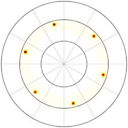
using high resolution transmission electron microscopy. Samples on MgO showed typical cube on cube epitaxial relationship NbN(001)[100]
|| MgO(001)[100], whereas samples on c-cut sapphire: NbN(111)[1![]() 0] || Al2O3(0001)[ 10
0] || Al2O3(0001)[ 10![]() 0]
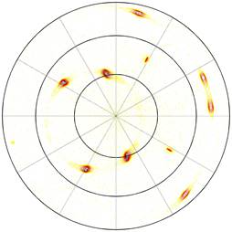
(Fig.1). For the case of r-cut Al2O3 substrate the pole
figures measured at 111NbN showed that the films are twinned and strongly oriented:
NbN(135) || Al2O3(10
0]
(Fig.1). For the case of r-cut Al2O3 substrate the pole
figures measured at 111NbN showed that the films are twinned and strongly oriented:
NbN(135) || Al2O3(10![]() 2) (Fig.2).
2) (Fig.2).
|
|
|
Figure 1. Pole figure in 200 NbN /c-cut Al2O3 . |
Figure 2. Pole figure in 111 NbN / r-cut Al2O3. |
|
|
|
1. A.D. Pogrebnjak, V.M. Rogoz, O.V. Bondar, N.K. Erdybaeva, S.V. Plotnikov, Protection of Metals and Physical Chemistry of Surfaces, 52, (2016), 802.
2. S. Volkov, M. Gregor, T. Roch, L. Satrapinskyy, B. Grančič, T. Fiantok, A. Plecenik, J. Electrical Engineering, (submitted 2019).
3. F. Mercier, S. Coindeau, S.Lay, A. Crisci, M. Benz, T. Encinas, R. Boichot, A. Mantoux, C. Jimenez, F. Weiss, E. Blonquet, Surface and Coatings Technology, 260, (2014), 126.
Authors would like to acknowledge a support by the Slovak Research & Development Agency under contract no. APVV-16-0315.