Pentacene growth on graphene by in situ GISAXS and GIWAXS
M. Jergel1, P. Šiffalovič1, P. Nádaždy1, M. Bodík1, E. Majková1, M. Hodas2, G. Duva2, B. Reisz2, F. Schreiber2, O. Konovalov3, W. Ohm4
1Institute of Physics SAS, Dúbravská cesta 9, 845 11
Bratislava, Slovakia
2Institut für
Angewandte Physik,
Universität Tübingen, Tübingen 72076, Germany
3European
Synchrotron Radiation Facility, Grenoble 38000, France
4Photon
Science, Deutsches Elektronen-Synchrotron
(DESY), Hamburg 22607, Germany
matej.jergel@savba.sk
Keywords: pentacene growth, graphene, epitaxy, GISAXS, GIWAXS
Abstract
Thin
films of small organic semiconducting molecules exhibit attractive optical and
electronic properties depending on their molecular structure. Pentacene (PEN) molecules
are known to form a lying-down phase on graphene that improves vertical electron
transport and increases optical absorption and light harvesting. Here, we
studied the mechanism of epitaxial PEN growth on graphene by in-situ GISAXS and
GIWAXS techniques complemented by ex-situ AFM and polarized confocal Raman
microscopy. Two principal stages of the growth were observed. First, nucleation
and growth of PEN islands saturating in width and height at 1 monolayer thickness
was observed. Later on, the islands continue to grow only
along [100] direction of the PEN triclinic lattice adopting needle-like shape and
copying hexagonal symmetry of the underlying graphene. The c* axis of PEN reciprocal
lattice was found to be parallel to the [210] (armchair) direction of graphene and
tilted by 18° with respect to the graphene surface. This suggests a »11° deviation
of the PEN molecular chains from the graphene surface driven by the energy
minimization in later stages of the islands growth.
Introduction
Thin films of small organic molecules are attractive for applications in light-emitting diodes, field-effect transistors or organic solar cells. The device performance critically depends on the molecular structure of the film which in turn depends on the substrate type. For the oxide surfaces such as SiO2, the standing-up configuration is typical. It the last decade it has been shown that templating the substrate with two-dimensional materials, the lying-down configuration can be achieved. Hence, this approach offers a possibility to control the molecular orientation and properties of the small molecule organic films. Indeed, the lying-down configuration of pentacene (PEN) molecules after evaporation on graphene was observed. PEN is an archetypal type of small organic molecules that are frequently used in organic electronics and photovoltaics. In order to optimize preparation of PEN films with the lying-down configuration, a study of the mechanism of PEN growth on graphene is needed. This gave impetus for the work presented here.
Experimental details
The PEN molecules (Sigma-Aldrich) were thermally evaporated onto epitaxially grown graphene on hexagonal 4H-SiC(0001) substrate (Graphensic) in a deposition chamber that was equipped with a beryllium window for the in-situ grazing-incidence small-angle and wide-angle X-ray scattering (GISAXS, GIWAXS) experiments. The deposition rate was 1.38 Å/min. The in-situ GISAXS/GIWAXS measurements were done at the 0.1° angle of incidence at ID10 (9.25 keV) and PO3 (11.4 keV) synchrotron beamlines at ESRF Grenoble and DESY Hamburg, respectively. Two hybrid pixel detectors acquired simultaneously and repeatedly the GIWAXS and GISAXS patterns during the evaporation (Maxipix and Pilatus 300K at ESRF, Pilatus 300K and Pilatus 1M at DESY). The 60 s integration time used at ESRF was reduced to 100 ms at DESY to capture initial stages of the deposition. The ex-situ GIWAXS measurements were done on a custom-designed Nanostar X-ray setup (Bruker AXS) equipped with a Ga liquid-metal jet anode X-ray source Excillum (9.25 keV) at an angle of incidence of 0.15° with a Pilatus 300K detector. The AFM measurements (Bruker, Dimension Edge) were done in tapping mode and the polarized Raman measurements were performed on a confocal Raman microscope (Witec, Alpha300 R+)
Results and conclusions
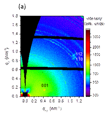
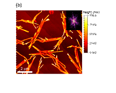
Figure 1. (a) GIWAXS pattern of PEN film and (b)
its AFM image with Fourier transform in the inset.
The ex-situ GIWAXS pattern after the PEN film deposition shows 3 diffraction spots (Fig. 1a). The film thickness calculated from the deposition rate and time corresponds to that of 10 PEN monolayers (MLs) reported previously [1]. The diffraction spots have no symmetric counterparts on the opposite side of the
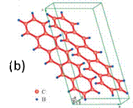
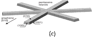
Figure 2. (a) Mutual orientation of PEN and
graphene lattices. (b) PEN unit cell and (c) crystallographic orientation of
PEN islands.
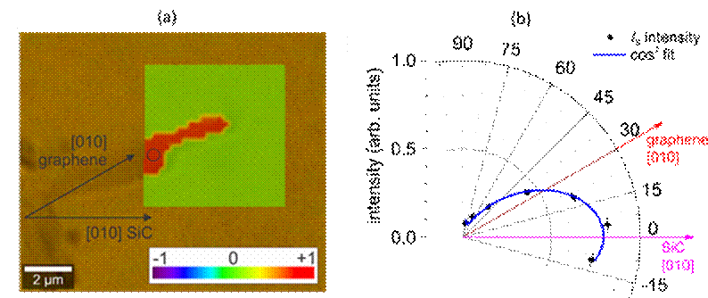
Figure 3. (a) Overlap of the optical and Raman
images of a PEN island and (b) cos2 fit of the azimuthal dependence
of Raman band integral intensity at 1373 cm‑1 (short molecular
axis vibrations) inside the black circle in (a).
pattern
(not shown) suggesting a monocrystalline structure of the film. It is composed
of PEN crystals forming needle-like islands that follow hexagonal symmetry of
the underlying graphene (Fig. 1b). The hexagonal unit cell of epitaxially
grown graphene on SiC is rotated by 30° from the SiC hexagonal unit cell. Supposing the triclinic PEN phase
[2], the orientation of PEN lattice with respect to graphene can be thus found
from the ex-situ GIWAXS pattern (Fig. 2a). The reciprocal c* axis of PEN
crystal is aligned along [210] (armchair) graphene direction and tilted by 18°
from the graphene surface. The crystallographic a axis of the PEN unit cell lies in the graphene
plane. Taking into account the PEN molecule orientation
in the unit cell (Fig. 2b), the long molecular axis does not follow the
[100] (zigzag) graphene direction but is tilted by 11°. This is due to energy
minimization in the presence of intermolecular interactions in
three-dimensional PEN crystals. The blurred ![]() and 112 diffraction spots
(Fig. 1a) originate from the crystals rotated by 120° and 300°
(Fig. 2c). The ex-situ polarized
confocal Raman microscopy revealed a uniform orientation of PEN
molecular chains inside the islands, confirming thus their monocrystalline structure
(Fig. 3).
and 112 diffraction spots
(Fig. 1a) originate from the crystals rotated by 120° and 300°
(Fig. 2c). The ex-situ polarized
confocal Raman microscopy revealed a uniform orientation of PEN
molecular chains inside the islands, confirming thus their monocrystalline structure
(Fig. 3).
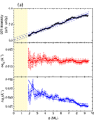
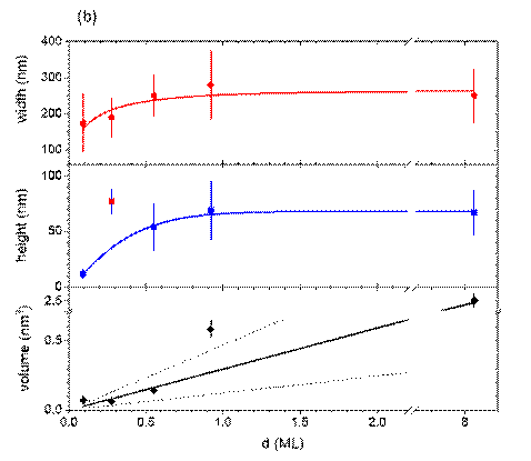
Figure 4. (a) Temporal evolution of PEN 001
diffraction peak parameters and (b) dimensions of PEN islands. (dots ‑ measured
points, lines – fits)
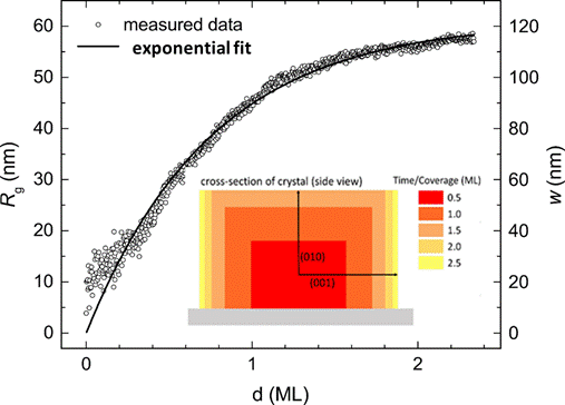
Figure 5. Temporal evolution of the radius of
gyration Rg
= ½ w (w – PEN islands width). The inset shows the growth of (100) facets.
The temporal evolution (in the number of deposited MLs) of the integral intensity of 001 diffraction extrapolated to zero thickness indicates a linear growth of the lying-down phase from the very beginning of deposition (Fig. 4a) when the scattered intensity was too low to be measured (yellow region). While the lateral Dqxy width of 001 diffraction spot is controlled by the limited resolution at grazing incidence, Dqz shows an increase in islands height from 25 nm to 44 nm between 2.5 and 8 MLs before the resolution limit is reached (Fig. 4a). The temporal evolution of the islands dimensions evaluated from AFM images taken ex-situ at selected deposition times suggests a strongly asymmetric growth due to the saturation of the islands width and height at 1 ML thickness (Fig. 4b). The asymmetry is driven by different surface energies of (001), (010) and (001) facets (Fig. 2c) that are 3.1, 4.8 and 6.4 meV/Å2, respectively.
The kinetics of PEN crystals growth was
studied by in-situ GISAXS. It could be measured simultaneously with GIWAXS as
the in-plane Bragg angle of 001 diffraction was slightly deviated from the
graphene zigzag direction (Fig. 2a). Due to the low PEN islands density
and large interisland distances exceeding experimental GISAXS resolution, the measured
GISAXS curve is primarily controlled by the interplay of three form factors corresponding
to three different crystal orientations (Fig. 2c). Hence, it could be evaluated
by Guinier analysis. As a
consequence of the highly anisotropic crystals growth, these form
factors contribute to GISAXS curve in different q ranges. Consequently, Guinier analysis
in a q range of (1÷2)×10‑3 Å‑1
allowed to analyze the temporal evolution of the radius of gyration which could
be attributed to a half of the islands width (Fig. 5). A fit with a simple exponential limited growth function provided a rate
constant of (3.5 ± 0.03)×10‑3 s-1. Combining these
results with AFM data, the
growth of (100) facets (Fig. 2c) can be visualized (inset in
Fig. 5).
Summarizing, a comprehensive time-resolved study of PEN thermal evaporation on a large-area graphene monolayer on SiC revealed a highly anisotropic epitaxial two-stage growth of a laying-down phase in the form of elongated islands following hexagonal symmetry of the substrate. The PEN islands posses triclinic monocrystalline structure, the long molecular axis being deviated from graphene by 11° in the final stage.
1. D. Nabok, P. Puschnig, C. Ambrosch-Draxl, O. Werzer, R. Resel, D.-M. Smilgies, Phys. Rev. B, 76, (2007), 235322.
2. C. C. Mattheus, A. B. Dros, A. J. Baas, A. Meetsma, J. L. de Boer, T. T. M. Palstra, Acta Crystallogr. C, 57, (2001), 939.
The
work was done during implementation of the project with ITMS code 26210120023 supported
by the Research and Development Operational Programme
funded by the ERDF.