Defect study in epitaxial SiGe graded microcrystals
M. Meduňa1, F. Isa2,3, A. Jung2,3, C.V. Falub2, A. Marzegalli4, M. Albani4, G. Isella5, K. Zweiacker, L. Miglio4, H. von Känel2,3
1Department of Condensed Matter Physics & CEITEC, Masaryk University, Brno, Czech Republic
2Laboratory for Solid State Physics, ETH-Zürich, Zürich, Switzerland
3Electron Microscopy Center, Empa, Dübendorf, Switzerland
4NESS, Department of Materials Science, Universita` di Milano-Bicocca, Milano, Italy,
5L-NESS, Department of Physics, Politecnico di Milano, Como, Italy
6Center for X-ray Analytics, Empa, Dübendorf, Switzerland.
mjme@physics.muni.cz
The defect free growth of various high-perfomance semiconductors on Si has been of high interest for many years. For Ge on Si, the mismatch of lattice (4.2 %) and thermal expansion coefficients (120.4 % at 300 K) leads to misfit dislocations (MDs) accompanied by threading dislocations (TDs) for layer thicknesses under critical value. Dislocations are a serious problem, since they negatively influence the performance of the devices. The thermal mismatch can even induce cracks in continuous heteroepitaxial layers depending on the growth temperature. These obstacles can be overcome by the heteroepitaxial growth on substrates patterned into a regular array of pillars at high aspect ratios [1] which eliminate the threading dislocation and cracks using the fast growth at out-of-equilibrium conditions. A very slow grading of Ge content in SiGe alloy from bottom of pillars up to their top [2] can eliminate the misfit dislocations. According to theory [3] a slow grading and a small base of the grown pillar can significantly eliminate misfit dislocations in highly mismatched, compositionally graded SiGe/Si heterostructures and this has been confirmed by our studies [2,4].
In this work we focus on compositionally graded heteroepitaxial SiGe microcrystals with different base size grown at grading rates from 1.5 to 6% µm-1. The microcrystals graded from 0 to 40% of Ge were investigated by a scanning X-ray nanodiffraction experiments performed at the ID01 beamline of the ESRF in Grenoble. Additionally the constant composition Ge microcrystals were measured with a standard high resolution X-ray diffraction in laboratory as well.
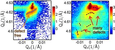
Figure 1. Example of details of the reciprocal space maps recorded close to the Si substrate peak close to the bottom of the crystal. (left) Pure elasticity is observed in the SiGe crystal with 2x2 µm base, (right) random plastic lattice bending is viewed as many irregular splits of the SiGe peak in the fast graded SiGe crystal.
Using 3D reciprocal space mapping and scanning X-ray diffraction microscopy together on the compositionally graded microstructures [5], we were able to reconstruct the microcrystal shape and lattice tilt inside individual microcrystals as 3D distribution [4]. We have found that in compositionally graded SiGe microcrystals the crystal lattice relaxes by convex bending since the misfit strain dominates [4] however in constant composition Ge microcrystals the lattice bending is concave due to pure thermal strain [6]. After a detailed analysis we could resolve formation of some crystal defects within the graded crystal growth according to crystal size and grading rate, see Figure 1, especially at the crystal bottom close to SiGe/Si interface.
We acknowledge the staff of the ID01 beamline at the ESRF,Grenoble, of the FIRST Center for Micro- and Nanoscience of ETH Zürich, and of EMEZ electron microscopy ETH Zürich.