X-ray characterization of thin layers
L. Horák
Department of Condensed Matter Physics, Faculty of Mathematics and Physics
horak@karlov.mff.cuni.cz
A layer can be defined as a material of single thickness covering a surface of a different material (called substrate). On the other hand, the meaning of the word thin is quite ambiguous in exact thickness limit. However, from an x-ray methods standpoint, it is quite reasonable to consider the thickness to be much smaller than the absorption length of x-ray radiation in a material. There are two reasons: Firstly, the volume of such layers is so small that experimental setting has to be adjusted to enhance the measured signal. Secondly, the primary beam and the scattered beam has to transmit through the surface of the layer, which restricts the geometry of the experiment, in other words, crystal cannot be rotated to arbitrary position.
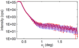
In the talk, we will give short overview of experimental setting, measurement and data evaluation of probably most common characterization techniques for thin layer. Firstly, the x-ray reflectivity is one of the exclusively surface techniques (for example see Figure 2). Since it is sensitive only to mean electron density in the sample, it can be successfully used for the study of amorphous, porous, polycrystalline, and even monocrystalline layers. It makes available information on the thickness of the layer, its relative density and the roughness of the surface and interfaces. It can be used not only for single layers, but it is powerful in determination of these parameters for the full stack of different sublayers. The maximal thickness is limited by the penetration depth that is quite low for low incident angle. On the other hand it can successfully detect a few nanometers thick oxide layer on the surface.
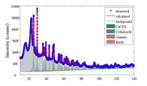
Polycrystalline thin layers as some coatings or active layers are usually studied using powder diffractometry in order to identify the crystallographic phases and other related parameters, e.g. grain sizes. Since the signal from the layer using usual Bragg-Brentano geometry is very weak, one has to use different geometry to enhance the layer signal. This can be achieved for instance using parallel beam geometry, in which the penetration depth is tuned by the angle of incidence (example in Figure 2).
|
|
|
Figure 2. Example of measured reflectivity curve fitted by the simulation. The thickness can be determined from the frequency of the oscillations. |
Figure 2. Standard powder pattern measured with fixed incidence angle to enhance the signal from the layer. |
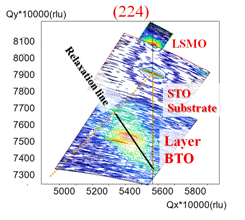
Thirdly, very often characterizing experiment for epitaxial thins layers is the determination of the lattice relaxation state. Using Reciprocal space mapping, one can very easily see if the layer lattice is laterally adjusted to the substrate lateral periodicity (co called pseudomorphic layers) or it is (partially) relaxed, i.e. the layer unit cell is not (fully) distorted with respect to its bulk prototype. This information come out from the comparison of the substrate peak positions with those of the layer. Figure 3 shows the example of BTO thin layer partially relaxed on LSMO pseudomorphically grown on STO substrate.
|
|
|
Figure 3. Reciprocal space map of asymmetric diffraction (224). The peak from pseudomorphic LSMO is located on the STO truncation rod, while the BTO peak is off this rod showing partial lattice relaxation. |
Figure 4. Measure intensity distribution along crystal truncation rods (red) is fitted by the simulation (blue). The interference between the wave diffracted in substrate and in the layer has to be taken into account. |
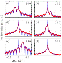
Lastly, we will show quite challenging task to determine the structure of the monocrystalline layer including atomic positions. It is not so straightforward using structure refinement from standard powder or monocrystal diffractometry. The main obstacle is; that the signal from the substrate is usually much stronger and it is overlapped with the signal from the layer. However, using high resolution diffractometry we can distinct the presence of the signal from the layer. Nevertheless, the substrate signal has to be necessarily incorporated into the structure solution, since we measure the interference pattern of these two signals. For example see Figure 4 which shows the interference pattern measured along several crystal truncation rods.