Diffraction surfaces in X-ray crystal monochromators prepared by nano-machining technique
Z. Zápražný1, D. Korytár1, Y. Halahovets2, M. Jergel2, C. Ferrari3, J. Hagara1,4, E. Dobročka1,
1Institute of Electrical Engineering, Slovak Academy of Sciences, Dúbravská cesta 9, 841 04 Bratislava, Slovakia
2Institute of Physics, Slovak Academy of Sciences, Dúbravská cesta 9, 845 11 Bratislava, Slovakia
3CNR-IMEM Institute, Parco Area delle Scienze 37/A, 431 24 Parma, Italy
4Integra TDS s. r. o., Pod Párovcami 4757/25, 921 01 Piešťany, Slovakia
zdenko.zaprazny@savba.sk
We study and develop methods for producing diffraction surfaces in X-ray crystal monochromators using advanced deterministic nano-machining technique [1]. Nano-machining uses a single point diamond tool to remove material from the surface. We have adopted two kinds of nano-machining techniques: Single point diamond turning (SPDT) and Fly cutting (grooving). The techniques are well developed for producing surfaces of infrared or visible light optics [2], however, their implementation for hard X-ray optics is a very challenging task. In a so called ductile mode, this technology is applicable even to brittle materials like germanium or silicon that are difficult to be machined, being only little invasive to crystal lattice beneath the surface. In particular, high-resolution TEM images have revealed absence of any dislocations in the subsurface region of the nano-machined Ge samples in the case of feed rate of 0.125 mm/min (Fig. 1).
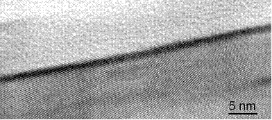
Figure 1. HR TEM image shows that the top surface is not perfectly flat as some valleys and crests of a few atomic layers depth/height with respect to an average surface occur. The perfect contact and sticking of the glue to the Ge sample excludes that such a roughness would be due to the removal of the very top atomic Ge layers by the Ar ion bombardment during the sample preparation. The Ge lattice terminates fully crystalline without any dislocations in the subsurface region.
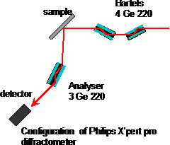
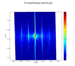
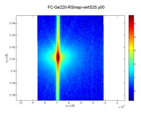
The crucial parameter is the surface roughness. The diamond tool produces periodical surface ripples, which can cause e.g. unwished parasitic interference effects in the case of hard X-ray radiation. HRXRD measurements showed that the periodicity of the ripples can vary from 700 to 40 nm depending on the used feed rate of nano-machining. Figure 2 shows a setup for the reciprocal space map (RSM) measurement of the Ge machined samples and channel-cut monochromator shown in Figure 3. The feed rate of nanomachining was 1 mm/min and the sample exhibits ripples with 416 nm periodicity (Figure 4). We have obtained very low surface roughness by optimizing of machining parameters and slowing down the feed rate to lower value of 0.125 mm/min. The truncation rods in reciprocal map were suppressed remaining only diffuse scattering indicating that the period of ripples after the tool is too short to observe using this HRXRD setup (Figure 5). By using of additional chemo-mechanical post-polishing process we have achieved the surface roughness (RMS) in the range of 1 - 0.3 nm according to AFM measurements. Applying SPDT nano-machining, it is possible to produce not only flat but also curved or free-form surfaces with very high accuracy. A high planarity of the diffraction surface down to 3nm/50µm has been achieved. This is very important due to a very small incidence or emergence angles of the hard X-ray beam in highly asymmetric channel- cut X-ray crystal monochromators [3].
|
|
|
|
Figure 2. RSM setup. High-resolution Philips diffractometer with a 3 bounce analyser crysta was used.l |
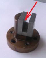
Figure 3. Artificial Ge channel-cut monochromator (assembled, glued together). The red arrow shows the machined inner side. |
|
|
|
|
Figure 4. The reciprocal space map shows vertical lines with a spacing 1.51x10⁻³ Å-1 corresponding to a planar spacing of 416 nm. |
Figure 5. RSM shows suppression of truncation rods present in Fig. 4. The diffuse scattering is present but limited. |
1. G.M. Robinson, M.J. Jackson: A review of micro and nanomachining from a materials perspective, Journal of Materials Processing Technology, Volume 167, Issues 2–3, 30 August 2005, Pages 316–337.
2. Robert E. Parks: Fabrication of infrared optics, Optical Engineering 33(3), 685—691 (March 1994).
3. C. Ferrari et al.: X-ray diffracted intensity for double-reflection channel-cut Ge monochromators at extremely asymmetric diffraction conditions, J. Appl. Crystallogr. 44, 353–358 (2011).
This work was done within Research and Development Centre for Advanced X-ray Technologies, ITMS code 26220220170, supported by the Research and Development Operational Program funded by the ERDF (0.5). This work was supported also by the Slovak Research Agency under the contracts No. APVV-14-0745 and Scientific Grant Agency of the Ministry of Education of Slovak Republic and the Slovak Academy of Sciences, project No. VEGA-2/0004/15.