Evaluation of threading dislocation density in III-nitride epitaxial layers
E. Dobročka
Institute of Electrical Engineering, Slovak Academy of Sciences, Dúbravská cesta 9,841 04 Bratislava, Slovak Republic
edmund.dobrocka@savba.sk
The III–nitride semiconductors of AlN, GaN, and InN and their
ternary alloys have great potential for use in optoelectronic and
high-temperature electronic devices due to their wide range of bandgaps and
high-temperature stability. The increasing range of
their applications such as light emitting diodes, lasers and high power
transistors requires the study of the influence of extended defects on the
electrical and optical properties of these materials
[1, 2]. The most important defects in the structures are threading dislocations
(TDs). Their total density in the epitaxial layers varies in the range from 108
to 1010 cm-2. They are predominantly oriented
perpendicularly to the sample surface as is proved by transmission electron
microscopy (TEM) observations. Three types of dislocations are generally
reported in these materials: a-type edge dislocations with Burgers vectors ![]() , c-type screw dislocations
with
, c-type screw dislocations
with ![]() and mixed a+c-type
dislocations with
and mixed a+c-type
dislocations with ![]() .
The density of edge dislocations, that are responsible
for lattice twisting within the plane of the sample, exceeds the density of
screw and mixed dislocations causing the lattice tilt out of the plane of the
layer.
.
The density of edge dislocations, that are responsible
for lattice twisting within the plane of the sample, exceeds the density of
screw and mixed dislocations causing the lattice tilt out of the plane of the
layer.
The dislocation density can be measured directly by TEM, but the
accuracy is rather poor due to the limited area covered by TEM micrographs. The
main significance of this technique is the possibility of determining the type
of the dislocations as well as the kind of their arrangement. Alternatively,
X-ray diffraction can be used to detect the lattice distortions caused by the
presence of dislocations averaged over a sufficiently large sample area. The
effect of lattice distortions on the diffraction peak broadening is well known
and there is a vast amount of literature dealing with this topic. While the
widths of the peaks can be measured by various X-ray diffraction techniques and
evaluated by fitting to different types of model curves, their interpretation
in terms of dislocation density is not straightforward. As regards the
measuring techniques, there is an important difference between polycrystalline
and single crystalline (epitaxial) samples. While in the former case a large
number of diffractions can be measured within one powder diffraction pattern
recorded e. g. in Bragg-Brentano set-up, measuring of (001) oriented single
crystals in symmetric configuration provides only diffractions ![]() that are sensitive to
lattice tilt and can therefore reveal only the presence of screw (eventually
screw component of mixed) TDs. The edge dislocations influence the lattice
planes perpendicular to the surface and measuring the corresponding
diffractions
that are sensitive to
lattice tilt and can therefore reveal only the presence of screw (eventually
screw component of mixed) TDs. The edge dislocations influence the lattice
planes perpendicular to the surface and measuring the corresponding
diffractions ![]() requires the grazing
incidence set-up.
requires the grazing
incidence set-up.
An alternative skew geometry enabling
to utilize the widths of diffractions ![]() that are inclined by an
angle
that are inclined by an
angle ![]() with respect to surface
normal was proposed by Sun et al. [3] and Lee et al. [4]. Their approach is
based on the model that supposes a mosaic structure of epitaxial films having a
large lattice mismatch [5]. The width
with respect to surface
normal was proposed by Sun et al. [3] and Lee et al. [4]. Their approach is
based on the model that supposes a mosaic structure of epitaxial films having a
large lattice mismatch [5]. The width ![]() of the diffraction
of the diffraction ![]() is given as
is given as
|
|
(1) |
where ![]() and
and ![]() are the FWHMs of the
diffractions
are the FWHMs of the
diffractions ![]() and
and ![]() , respectively,
, respectively, ![]() is the lateral domain size and
is the lateral domain size and ![]() is the magnitude of the
diffraction vector. The exponent
is the magnitude of the
diffraction vector. The exponent ![]() varies between 1 (Lorentzian intensity profile) and 2 (Gaussian
profile). The third term in (1) corresponds to the size broadening effect that
in some cases has to be taken into account.
varies between 1 (Lorentzian intensity profile) and 2 (Gaussian
profile). The third term in (1) corresponds to the size broadening effect that
in some cases has to be taken into account.
Measuring of at least one symmetric (at ![]() ) and one skew diffraction
at
) and one skew diffraction
at ![]() enables one to obtain the
extrapolated value of
enables one to obtain the
extrapolated value of ![]() corresponding to twist of
the mosaic blocks due to the presence of edge TDs.
corresponding to twist of
the mosaic blocks due to the presence of edge TDs.
In the vast majority of analyses of the quality of epitaxial layers
the formulas originally derived for polycrystalline metallic samples are used
for evaluation of the TDs densities from the diffraction peak widths [6-8]. Two
limiting cases are distinguished: (i) random distribution of TDs, in which the
dislocation density ![]() is related to peak width
is related to peak width ![]() as
as
|
|
(2) |
and (ii) correlated distribution when the dislocations are localized at the boundaries of mosaic blocks
|
|
(3) |
where ![]() is the magnitude of
Burgers vector and
is the magnitude of
Burgers vector and ![]() is the average size of
the blocks. It is worth noting that for polycrystalline samples the formulas
(2) and (3) do not provide the possibility to distinguish between screw and
edge dislocations. In order to solve this problem more sophisticated approaches
are required [9, 10] that take into consideration the mutual orientation of the
dislocation line, possible Burgers vectors and diffraction vectors and
eventually the crystal anisotropy. These complications are considerably reduced
for epitaxial layers, where only one direction of TDs and, in principle, only
two types of Burgers vectors have to be considered. Setting the values of
is the average size of
the blocks. It is worth noting that for polycrystalline samples the formulas
(2) and (3) do not provide the possibility to distinguish between screw and
edge dislocations. In order to solve this problem more sophisticated approaches
are required [9, 10] that take into consideration the mutual orientation of the
dislocation line, possible Burgers vectors and diffraction vectors and
eventually the crystal anisotropy. These complications are considerably reduced
for epitaxial layers, where only one direction of TDs and, in principle, only
two types of Burgers vectors have to be considered. Setting the values of ![]() and
and ![]() for the peak widths
for the peak widths ![]() in (2) or (3) and using the appropriate magnitudes of Burgers
vectors
in (2) or (3) and using the appropriate magnitudes of Burgers
vectors ![]() and
and ![]() , one can easily calculate
the density of screw and edge dislocations. The results evidently depend on the
supposed dislocation arrangement that has to be
verified e. g. by TEM observation along with the estimation of the parameter
, one can easily calculate
the density of screw and edge dislocations. The results evidently depend on the
supposed dislocation arrangement that has to be
verified e. g. by TEM observation along with the estimation of the parameter ![]() .
.
More precise approach based on the analysis of the shape of the
rocking curves was proposed by Kaganer and co-workers [11, 12]. They fit the
measured intensities by the numerical Fourier transformation of the correlation
function proposed by Krivoglaz [9] in the whole range of rocking curves
including the peak tails. In addition to dislocation density, the model allows
to extract also the so called cut-off radius ![]() . This parameter was
introduced by Wilkens [12] in order to characterize the correlation of dislocations
within the framework of “restricted random distribution” model. Its value gives
the size of the domains within which the dislocation distribution is random
(the sum of all Burgers vectors in the domain is zero). However, the
application of this model is rather laborious and not suitable for everyday use
by technologists. For practical purposes approximate formulas were derived on
the basis of this model [11] in the forms
. This parameter was
introduced by Wilkens [12] in order to characterize the correlation of dislocations
within the framework of “restricted random distribution” model. Its value gives
the size of the domains within which the dislocation distribution is random
(the sum of all Burgers vectors in the domain is zero). However, the
application of this model is rather laborious and not suitable for everyday use
by technologists. For practical purposes approximate formulas were derived on
the basis of this model [11] in the forms
|
|
(4) |
for edge dislocations and
|
|
(5) |
for screw ones. ![]() is the Bragg angle of the
measured diffraction and the dimensionless parameter
is the Bragg angle of the
measured diffraction and the dimensionless parameter ![]() depending on the
corresponding TDs densities
depending on the
corresponding TDs densities ![]() varies between 1 and 2.
Surprisingly, compared to (2), these equations result in four times higher edge
dislocation density and an order higher screw dislocation density [11].
varies between 1 and 2.
Surprisingly, compared to (2), these equations result in four times higher edge
dislocation density and an order higher screw dislocation density [11].
It is seen that there is a large discrepancy between different
approaches to the evaluation of TDs densities. While the dependence ![]() for random distribution is
generally accepted, the numerical factor can considerably vary, eventually
depends on dislocation densities. This uncertainty can be partially excluded by
comparison of the results with the TEM observation, although the precision of dislocation
density measurement by TEM is rather low. Once the ratio
for random distribution is
generally accepted, the numerical factor can considerably vary, eventually
depends on dislocation densities. This uncertainty can be partially excluded by
comparison of the results with the TEM observation, although the precision of dislocation
density measurement by TEM is rather low. Once the ratio ![]() is established for a
given type of epitaxial system (and eventually laboratory), the calibration can
be used for further XRD analyses. This procedure was applied for the evaluation
of TDs in InN layers grown on GaN [13]. The densities of both screw and edge TDs
were calculated according to
is established for a
given type of epitaxial system (and eventually laboratory), the calibration can
be used for further XRD analyses. This procedure was applied for the evaluation
of TDs in InN layers grown on GaN [13]. The densities of both screw and edge TDs
were calculated according to
|
|
(6) |
where 1.88 is the calibration constant obtained from the comparison with TEM.
In this contribution the TDs density was evaluated in both layers of
InN/GaN/sapphire(0001) sample. The InN and GaN layers were 0.5 μm and 0.3
μm thick, respectively. The details of the growth procedure are described
elsewhere [14]. High resolution X-ray diffraction
analysis was carried out using Bruker D8 DISCOVER diffractometer equipped with
X-ray tube with rotating Cu anode operating at 12 kW. The measurements were
performed with parabolic Goebel mirror and four-bounce Ge 022 Bartels
monochromator in the primary beam. All diffraction curves were recorded in an
open detector mode. The InN layer on GaN was fully relaxed as confirmed by
measuring of one asymmetric ![]() diffraction. The density
of dislocations with screw and edge components in both InN and GaN layers was
evaluated from the X-ray rocking curves. FWHMs of two symmetric diffraction –
diffraction. The density
of dislocations with screw and edge components in both InN and GaN layers was
evaluated from the X-ray rocking curves. FWHMs of two symmetric diffraction – ![]() ,
, ![]() and three skew ones –
and three skew ones – ![]() ,
, ![]() and
and ![]() were determined. Four of
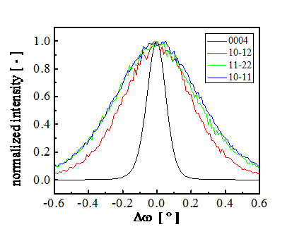
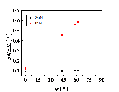
them are shown for InN layer in Fig. 1. Comparison of the peak widths of the
same diffractions for InN and GaN are shown in Fig. 2. It is seen that for InN layer the peak broadening
systematically increases with the tilting angle
were determined. Four of
them are shown for InN layer in Fig. 1. Comparison of the peak widths of the
same diffractions for InN and GaN are shown in Fig. 2. It is seen that for InN layer the peak broadening
systematically increases with the tilting angle ![]() indicating that the
density of edge TDs exceeds the density of screw ones. On
the contrary, the peak widths practically do not change for GaN layer.
indicating that the
density of edge TDs exceeds the density of screw ones. On
the contrary, the peak widths practically do not change for GaN layer.
|
|
|
Figure 1. Normalized X-ray rocking curves of selected diffractions of InN. |
Figure 2. Dependence of
FWHMs of rocking curves on the tilting angle
|
The TDs
densities ![]() and
and ![]() were calculated according
to (6), where the FWHMs of rocking curves
were calculated according
to (6), where the FWHMs of rocking curves ![]() and
and ![]() at the inclination angle
at the inclination angle ![]() and at the extrapolated
value
and at the extrapolated
value ![]() were set for the
parameter
were set for the
parameter ![]() . Gaussian type of rocking curves was supposed, hence the exponent
. Gaussian type of rocking curves was supposed, hence the exponent ![]() was used in (1) for
calculation of
was used in (1) for
calculation of ![]() . The size effect (third term in (1)) was neglected in the calculation. The values of the tilting angle
. The size effect (third term in (1)) was neglected in the calculation. The values of the tilting angle ![]() for skew diffractions
were calculated from the lattice parameters of InN (PDF 00-050-1239) and GaN (PDF 00-050-0792).
The magnitudes of Burgers vectors
for skew diffractions
were calculated from the lattice parameters of InN (PDF 00-050-1239) and GaN (PDF 00-050-0792).
The magnitudes of Burgers vectors ![]() and
and ![]() are equal to the lattice
parameters
are equal to the lattice
parameters ![]() and
and ![]() , respectively, for both
hexagonal materials.
, respectively, for both
hexagonal materials.
The obtained TDs
densities are ![]() ,
, ![]() ,
, ![]() and
and ![]() . For both layers the same
value 1.88 of the calibration constant was used in (6). Generally, one should
be cautious with the choice of calibration proposed by different authors. The
ratio
. For both layers the same
value 1.88 of the calibration constant was used in (6). Generally, one should
be cautious with the choice of calibration proposed by different authors. The
ratio ![]() may vary significantly
from 0.1 to 7 as summarized in [4]. But in spite of this uncertainty, the
increase of the density of edge TDs in the InN layer in comparison to GaN is
evident. While the density of screw dislocations is practically the same, new
edge TDs are generated during the growth of InN layer and their density exceeds
the density of edge TDs “coming” from GaN layer by more than one order of
magnitude. This is probably caused by large mismatch between the GaN and InN
lattices that is ~ 10% for fully relaxed InN layer.
may vary significantly
from 0.1 to 7 as summarized in [4]. But in spite of this uncertainty, the
increase of the density of edge TDs in the InN layer in comparison to GaN is
evident. While the density of screw dislocations is practically the same, new
edge TDs are generated during the growth of InN layer and their density exceeds
the density of edge TDs “coming” from GaN layer by more than one order of
magnitude. This is probably caused by large mismatch between the GaN and InN
lattices that is ~ 10% for fully relaxed InN layer.
The analyzed samples were rather thick and the corresponding diffractions of InN and GaN were well separated even in the skew geometry used in the experiment. This is due to the large difference between the lattice parameters of these materials. However, one can encounter some difficulties when attempting to measure the TDs densities in multilayered ternary compounds having similar lattice parameters. The use of analyser crystal instead of open detector system can improve the resolution, however, this modification can seriously decrease the intensity. This is particularly important if the measurement should be performed on samples with the layer thicknesses in the range of tens of nanometers. These values are typical for up-to-date technologies. As regards the calculated TDs densities, one should reconcile oneself to the fact that the precision of density evaluation is seriously limited. This is not caused by the possible error of measurement but is rather a consequence of the fact that each model intended to describe the dislocation distribution is too far from reality.
1. S. C. Jain, M. Willander, J. Narayan, J. Appl. Phys., 87, (2000), 965.
2. W. V. Lundin, A. E. Nikolaev, A. V. Sakharov, S. O. Usov, E. E. Zavarin, P. N. Brunkov, M. A. Yagovkina, N. A. Cherkashin, A. F. Tsatsulnikov, Semiconductors, 48, (2014), 53.
3. Y. J. Sun, O. Brandt, T. Y. Liu, A. Trampert, K. H. Ploog, Appl. Phys. Lett. 81, (2002), 4928.
4. S. R. Lee, A. M. West, A. A. Allerman, K. E. Waldrip, D. M. Follstaedt, P. P. Provencio, D. D. Koleske, and C. R. Abernathy, Appl. Phys. Lett. 86, (2005), 241904.
5. V. Srikant, J. S. Speck, D. R. Clarke, J. Appl. Phys. 82, (1997), 4286.
6. P. Gay, P. B. Hirsch, A. Kelly, Acta Metall. 1, (1953), 315.
7. C. G. Dunn, E. F. Koch, Acta Metall. 5, (1957), 548.
8. R. Chierchia, T. Böttcher, H. Heinke, S. Einfeldt, S. Figge, D. Hommel, J. Appl. Phys. 93, (2003), 8918.
9. M. A. Krivoglaz, X-ray and Neutron Diffraction in Nonideal Crystals. Berlin: Springer-Verlag, 1996.
10. R. Kužel, Z. Kristallogr. 222, (2007), 136.
11. V. M. Kaganer, O. Brandt, A. Trampert, and K. H. Ploog, Phys. Rev. B,72, (2005), 045423.
12. V. S. Kopp, V. M. Kaganer, M. V. Baidakova, W. V. Lundin, A. E. Nikolaev, E. V. Verkhovtceva, M. A. Yagovkina, N. Cherkashin, J. Appl. Phys. 115, (2014), 073507.
13. C. S. Gallinat, G. Koblmüller, Feng Wu, J. S. Speck, J. Appl. Phys. 107, (2010), 053517.
14. Ch. Zervos, A. Adikimenakis, P. Beleniotis, A. Kostoupolos, M. Kayambaki, K. Tsagaraki, G. Konstantinidis, A. Georgakilas, Appl. Phys. Lett. 108, (2016), 142102.
The author gratefully acknowledges A. Georgakilas and A. Adikimenakis from FORTH, Greece for providing the sample.