Energetic ion beams for compositional and structural study of crystalline materials for optics and photonics
A. Macková1,2, P. Malinský1, R. Mikšová1,2, H. Pupíková1,2, A. Jágerová1,2, R. Böttger3
1Nuclear Physics Institute of the Czech Academy of Sciences, v. v. i., 250 68 Rez, Czech Republic
2Department of Physics, Faculty of Science, J. E. Purkinje University, Ceske Mladeze 8, 400 96 Usti nad Labem, Czech Republic
3Institute of Ion Beam Physics and Materials Research, Helmholtz Zentrum Dresden-Rossendorf, 01328 Dresden, Germany
mackova@ujf.cas.cz
Energetic ion beam serve as a versatile analytical tool for compositional characterization of all types of materials and structures including structural studies applying Rutherford Back-Scattering spectrometry (RBS) in channeling mode on crystalline materials. Energetic ion beams can be used either as an analytical tool or as deposition technique for nano and microstructure synthesis for wide range of material application as electronics, optics, spintronics, biomedicine etc. [1 -3]. RBS channeling method is based on the charged particle channeling in the periodic potential of crystalline atom rows. The penetrating ion beam is focused to the forward direction and the back-scattering probability decreases significantly, thus the yield of the back-scattered ions in the spectra is a descending function of the incoming ion beam angle; see an example of the visualized crystal by ion beam in Figure 1 on the left [4]. Following the back-scattered ion yield in dependence to the incoming angle of ions gives us information about the impurity atoms positions, disordered atoms in the interstitials positions, displacement atoms density and its depth profiles etc. Fundamental studies focused on ion beam penetration through the single crystalline samples in different crystallographic orientation and their energy stopping can be provided also which topic is very rarely reported in literature [5]. First information concerning dopant depth profiles, the surface layer composition and relative disordered atom number in surface layer can be easily derived from the aligned spectrum (ion beam is aligned along the main crystallographic axis and back-scattered ions are recorded) and the random spectrum (ion beam impinges randomly on the sample which is realized by the automatized two axis rotational procedure of the investigated sample during the measurement).
The advanced precise information about the investigated structural changes can’t be provided without the MC simulation, where the binary collisions approximation with the close encounter probability calculation is used. FLUX is a batch of routines, which enables to simulate ion flux (see Figure 1 on the right), ion momentum and energy for the various crystallographic orientations, enables to generate the spectrum of back-scattered ions in dependence of the incoming ion beam angle (angular scans).
Nano-structure deposition using ion implantation technique is very promising technology nowadays. Rare earth and metal ion implantation into crystalline materials (LiNbO3, sapphire, ZnO, GaN) serves as a progressive way to develop new materials with the extraordinary optical, luminescent and/or magnetic properties [6-10]. The presented contribution includes several examples of the nano-structures prepared by means of the ion implantation in above mentioned crystalline materials, the characterization of prepared nanostructures by RBS and RBS channeling to get the compositional and structural information in connection to complementary methods as XRD, Raman spectroscopy and to the functional properties (optical, luminescent and magnetic properties) [6-8].
The above mentioned problematics is realized at the CANAM (Center of Accelerators and Nuclear Analytical Methods) infrastructure LM 2011019 in collaboration with Institute of Chemical Technology in Prague, Helmholtz Zentrum Dresden-Rossendorf, Germany and Peter Grünberg Institut, Forschungszentrum Jülich, Germany, where the complementary analyses were provided.
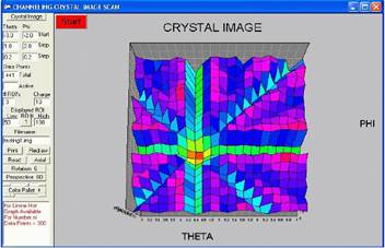
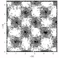
Figure 1 RBS channeling crystal image visualized by He+ 2 MeV ion beam on the left and MC FLUX simulation of transmitting ion beam through <100> silicon crystal.
1. A.J. Kenyon, Prog. Quant. Electron. 26, (2002), 225.
2. T. Dietl, Phys. Status Solidi B 240, (2003), 433.
3. A. Mackova, P. Malinsky, B. Svecova, P. Nekvindova, R. Groetzschel, Nucl. Inst. Meth. B, 268 (2010), 2047-2050.
4. Ion Beam Analysis, M. Nastasi, J. W. Mayer, and Y. Wang, Taylor and Francis, Boca Raton, USA, 2015.
5. R. Miksova, R., V. Hnatowicz, A. Mackova, A. et al., Nucl. Inst. Meth. B, 354, (2015), 205-209
6. Z. Sofer, D. Sedmidubsky, M. Moram, A Mackova, M. Marysko, J. Hejtmanek, C. Buchal, H. Hartdegen, M.Vaclavu,V. Perina, R. Groetzschel, M. Mikulics, Thin Solid Films, 519 (2011) 6120-6125
7. A. Mackova, P. Malinsky, Z. Sofer, P. Simek, D. Sedmidubsky, M. Mikulics, and R. A. Wilhelm, Nucl. Inst. Meth. B, 307, (2013), 446–451.
8. A. Macková, P. Malinsky, Z. Sofer, P. Šimek, D. Sedmidubsky, M. Vesely, and R. Böttger, Nucl. Inst. Meth. B 371, (2016), 254–257.
9. M. Mikulics, Y. C. Arango, A. Winden, R. Adam, A. Hardtdegen, D. Grützmacher, E. Plinski, D. Gregušová, J. Novák, P. Kordoš, A. Moonshiram, M. Marso, Z. Sofer, H. Lüth, and H. Hardtdegen, Appl. Phys. Lett. 108, (2016), 061107.
10. L. M. C. PereiraJ. P. AraújoU. WahlS. DecosterM. J. Van BaelK. Temst,A. Vantomme,J. Appl. Phys. 113, (2013) 023903.