Strain relaxation in Ge microcrystals studied by X-ray diffraction
J. Rozbořil1, M. Meduňa1, C.V. Falub2, F. Isa2, H. von Känel2
1Department of Condensed Matter Physics & CEITEC, Masaryk University, Kotlářská 2, 61137 Brno, Czech Republic
2Laboratory for Solid State Physics, ETH-Zürich, Schafmattstrasse 16, 8093 Zürich, Switzerland
jj.rozboril@gmail.com
Monolithical integration of different material layers is increasingly required during fabrication process of modern semiconducting optical and electronical devices. Keeping heterostructures strain and defect free is of course one of the conditions for proper functionality of devices and it could be problematic when materials with different lattice parameters and different coefficients of thermal expansion are matched. Epitaxial growth of layer on a substrate, which lattice parameter does not match with the lattice parameter of the layer, usually leads to a creation of misfit and threading dislocations arising from the interface. Different coefficients of thermal expansion of the layer and substrate causes bowing or even cracks of the heterostructure, when its temperature changes.
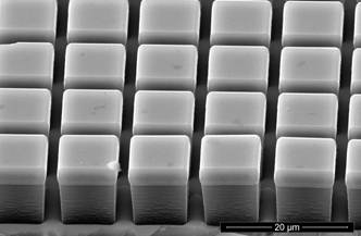
A promising method of dealing with those obstacles involves patterning of the substrate into a periodic array of pillars and a deposition with relatively high deposition rate [1]. The resulting heterostructure consists of separated microcrystals grown on the top of each substrate pillar, see Fig. 1. Dislocations created at the interface of layer and substrate are localized only at the bottom part of microcrystals because of high aspect ratio of microcrystals.
In this work, we have studied series of samples of Ge microcrystals deposited by Low-Energy Plasma-Enhanced Chemical Vapor Deposition (LEPECVD) on a Si substrate, which was patterned into the rectangular array of 8 μm tall square based pillars using conventional photolithography and deep reactive ion etching. The studied samples differed in the latteral size of Si pillars varying from 2 μm to 15 μm, and in the size of the trench between two neighbouring Si pillars varying from 1 μm upto 50 μm for different samples.
For the analysis, we have used home assembled diffractometer with a Cu x-ray tube equipped with a Göbel parabolic graded multilayer mirror and a 4-bounce Ge(220) crystal monochromator, providing Cu Kα1 radiation on the incident beam, and an analyzer crystal on the diffracted beam in order to perform high resolution x-ray diffraction measurements using reciprocal space mapping around symmetrical (004) and asymmetrical (224) diffraction.
We have proved by analyzing diffraction peak positions and their intensity that the Ge forming microcrystals is completely relaxed up to the lateral size of 9 μm whereas the Ge deposited into the trenches is tensile strained.
In order to investigate the dependency of the Ge layer crystal quality on the structure parameters of the substrate patterning, we have analyzed Ge diffraction peak half-widths as well. We have found that the thermal strain plays a dominant role in the diffraction peaks broadening. The diffraction peaks are narrowing with decreasing trench size probably due to the reduction of the areas of the Ge microcrystals extending Si pillars. The samples with 5 × 5 μm2 sized Si pillars exhibit the most significant lattice bending from all of the measured samples.
|
|
| Figure 1. Perspective view SEM micrograph of 3 μm tall Ge microcrystals grown on Si substrate with 8 μm tall and 9 μm wide pillars, spaced by 3 μm gaps. |
1. C.V. Falub, H. von Känel, F. Isa, R. Bergamaschini, A. Marzegalli, D. Chrastina, G. Isella, E. Müller, P. Niedermann, L. Miglio, Science, 335, (2012), 1330-1334.