Reconstruction of crystal shapes by X-ray nanodiffraction from 3D multiple quantum wells
M. Meduňa1, C.V. Falub2, F. Isa3, D. Chrastina3, T. Kreiliger2, G. Isella3, H. von Känel2
1Department of
Condensed Matter Physics & CEITEC, Masaryk University, Kotlářská 2, 61137
Brno, Czech Republic
2Laboratory for Solid State Physics, ETH-Zürich, Schafmattstrasse
16, 8093 Zürich, Switzerland
3L-NESS, Department of Physics, Politecnico di Milano, via Anzani
42, 22100 Como, Italy mjme@physics.muni.cz
Advances in focusing of X-rays during past years have allowed tremendous increase in spatial resolution of scattering techniques. In this work we show that scanning sub-micrometer diffraction using focused synchrotron radiation can unravel the three-dimensional structure of epitaxial crystals containing a periodic multiple quantum wells underneath their faceted surface.
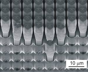
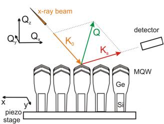
As an example we use 8 micron high SiGe crystals (Ge content 90%) grown by low-energy plasma enhanced chemical vapor deposition (LEPECVD) on a regular array of Si pillars etched deep into the Si substrate. The SiGe crystals are monolitically formed by self limited lateral growth [1] into the shape of high, 3D faceted towers as a buffer for final growth of multilayer on top, see Figure 1. These SiGe microcrystals are further conformal overgrown by a periodical Ge/SiGe multiple quantum well (MQW) structure [2], see scheme in Figure 2. This allows amplification of the truncution rod diffraction from every part of the surface. For a nanodiffraction experiment the neighbouring crystals were isolated in order to detect the signal only from one individual crystal [3].
The X-ray nanodiffraction experiment was performed at the ID01 beamline of the European Synchrotron Radiation facility (ESRF) in Grenoble. The beam was focused down to 500 nm using a Fresnel zone plate (FZP) and scanned over the sample by a piezo stage, see Figure 2. By mapping reciprocal space using 2D pixel detector, three-dimensional reciprocal space maps (RSMs) were constructed for each (x,y) position of the x-ray beam on the sample. Since the microcrystal surface with facets, see Figure 3a, was covered by MQW, the diffracted intensity was aligned into MQW satellites in reciprocal space ordered along four truncation rods each perpendicular to irradiated surface, see Figures 3d,e,f. A cut through isointensity plot of 3D RSM is shown in Figure 3c.
|
|
|
Figure 1. SEM image of epitaxial grown 8 mm high Ge crystals grown on 8 mm high Si pillars, see Ref. [4]. |
Figure 2. Schematic sketch of scattering geometry with incident beam K0 and exit beam Ks defining the scattering vector Q, see Ref. [4]. |
If we limit the detected intensity only to selected MQW satellite peaks, the diffraction signal is sensitive only to particular surface corresponding to selected facet. Thus using this scanning diffraction technique, we can map shape of individual facets. In Figure 3b, the (x,y) mesh of total intensity collected around all SL-1 peaks is plot and it clearly shows the shape of {113} crystal facets on top. If only peaks from one truncation rod are selected, the mesh will image only the one corresponding facet. This type of imaging in Figure 3b well correlates with the SEM image in Figure 3a, observed from the same viewing angle as the incidence angle of x-ray beam.
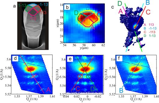
Figure 3. Perspective SEM micrograph view of 8 μm tall Ge crystal with significant crystallographic facets, A (113), B (-1-13), C (-113), D (1-13). (a). The intensity mesh from all SL-1 peaks shows the complete shape of crystal surface covered by diffracting MQW structure (b). 3D isolevel plot of the scattered intensity cut in the middle shows all four ABCD truncation rods (c). Examples of (Qx,Qz) 3D RSM projections around SiGe (115) reciprocal lattice point recorded at facet A (113) (d) and B (-1-13) (f). The projection of 3D RSM into (Qy,Qz) plane shows truncation rods from both facets C (-113) and D (1-13) (e), see Ref. [4].
Using this method we could determine also the MQW properties on top of each individual crystal facet depending on the beam position [4]. From the diffraction peak shape we could map the very high crystalline quality of the structure as well. The presence of the MQW allows the reconstruction of the crystal shape without the need of any structural model.
We acknowledge the staff of ID01 beamline at ESRF; the FIRST Center for Micro- and Nanoscience of ETH Zürich for making available its infrastructure and helpful discussions with B. Batlogg and A. Dommann.
1. C.V. Falub, H. von Känel, F. Isa, R. Bergamaschini, A. Marzegalli, D. Chrastina, G. Isella, E. Müller, P. Niedermann, L. Miglio, Science, 335, (2012), 1330.
2. F. Pezzoli, F. Isa, G. Isella, C.V. Falub, T. Kreiliger, M. Salvalaglio, R. Bergamaschini, E. Grilli, M. Guzzi, H. von Känel, L. Miglio, Phys. Rev. Applied, 1, (2014), 044005.
3. C. V. Falub, M. Meduňa, D. Chrastina, F. Isa, A. Marzegalli, T. Kreiliger, A.G. Taboada, G. Isella, L. Miglio, A. Dommann, and H. von Känel, Scientific Reports 3 (2013), 2276.
4. M. Meduňa, C.V. Falub, F. Isa, D. Chrastina, T. Kreiliger, G. Isella, H. von Känel, J. Appl. Cryst., 47, (2014), 2030.