Structural properties of epitaxial Ge microcrystals on Si
J. Rozbořil1, M. Meduňa1, C.V. Falub2, F. Isa3, G. Isella3,
H. von Känel2
1Department of Condensed Matter Physics & CEITEC, Masaryk University, Kotlářská 2, 61137 Brno, Czech Republic
2Laboratory for Solid State Physics, ETH-Zürich, Schafmattstrasse 16, 8093 Zürich, Switzerland 3L-NESS, Department of Physics, Politecnico di Milano, via Anzani 42, 22100 Como, Italy
357604@mail.muni.cz
The fabrication of modern semiconducting optical devices requires combining of different materials. Heteroepitaxial growth of layers with different lattice parameters and thermal expansion coefficients generates many obstacles during fabrication, in particular, creation of misfit and threading dislocations in the deposited layer and cracks, which detrimentally affect the fabricated device. One of the main applications of Ge/Si heteroepitaxial thick layers can be a development of new generation of x-ray detectors.
Successful method of fabricating defect-free epitaxial Ge/Si layers involves patterning of the Si substrate into periodic arrays of pillars by a conventional photolithography and deep reactive ion etching, on which germanium layer is deposited by Low-Energy Plasma-Enhanced Chemical Vapor Deposition (LEPECVD) at high growth rate [1]. Separated relaxed Ge microcrystals with defects localized only in a small area around Ge/Si interface, which doesn’t affect bulk properties, can be a solution (Fig. 1). The crystals can be grown up to height of several tens of micrometers and the material deposited can result in space filling even up to 96 % of surface.
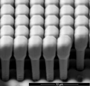
Figure 1. Perspective view SEM micrograph of 8 μm tall Ge microcrystals grown on Si substrate with 8 μm tall and 2 μm wide pillars, spaced by 2 μm gaps.
Series of Ge microcrystal samples grown on Si substrate with different structure parameters were studied by high-resolution x-ray diffraction technique using reciprocal space mapping around symmetrical (004) and asymmetrical (224) diffractions. We have used home assembled diffractometer with a Cu x-ray tube equipped with a 4-bounce Ge(220) crystal monochromator on the incident beam and an analyzer crystal on the diffracted beam, providing Cu Kα1 radiation.
Two significant Ge diffraction peaks on the measured maps are clearly observed (Fig. 2). The first one refers to strained germanium deposited inside the trenches between the Si pillars and the second one refers to germanium deposited on the top of the Si pillars, which is completely relaxed. The intensity of both kinds of peaks and also their width strongly depend on the structure of the samples, patterning, height etc.
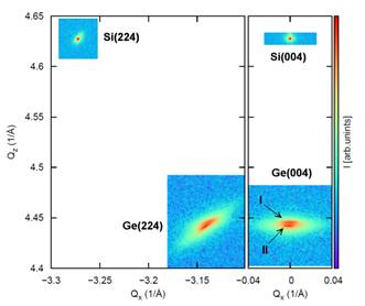
Figure 2. Reciprocal space maps around 224 (left) and 004 (right) diffractions for sample of 3 μm tall Ge microcrystals grown on Si substrate with 8 μm tall and 2 μm wide pillars, spaced by 3 μm gaps. Peak I-strained Ge between pillars; peak II-relaxed Ge towers.
Particularly in this study we compare samples which differ from each other in Ge crystal height, size of the Si pillars and distances between them. The Ge crystal height varies in the range from 1 to 30 μm. The Si pillars on a substrate have square cross-section and they are arranged in a square grid. The Si pillars are 8 μm tall on all samples, their widths are in the range from 2 to15 μm and they are spaced with the gaps varying from 1 to 50 μm. The crystal lattice properties such as lattice parameter, tilt, strain and degree of relaxation and their dependence on the sample patterning were studied using intensity, FWHM and position of diffraction peaks.
1. C.V. Falub, H. von Känel, F. Isa, R. Bergamaschini, A. Marzegalli, D. Chrastina, G. Isella, E. Müller, P. Niedermann, L. Miglio, Science, 335, (2012), 1330-1334.
2. C. V. Falub, M. Meduňa, D. Chrastina, F. Isa, A. Marzegalli, T. Kreiliger, A.G. Taboada, G. Isella, L. Miglio, A. Dommann, and H. von Känel, Scientific Reports 3 (2013), 2276.