Growth and structure of thin films of organic semiconductors: a real-time in situ GISAXS study
C.
Frank1, J. Novák1, R. Banerjee1, A. Gerlach1,
F. Schreiber1, A. Vorobiev2,
J. Banerjee3, and S. Kowarik3
1Institut
für Angewandte Physik, Eberhard Karls Universität Tübingen,
Auf der Morgenstelle 10,
72076 Tübingen, Germany
2European Synchrotron Radiation Facility, 6 Rue Jules Horowitz, BP 220, 38043 Grenoble Cedex 9, France
3Institut für Physikalische und Theoretische Chemie, Universität Tübingen,
Auf der Morgenstelle 18, 72076 Tübingen, Germany
4Institut für Physik, Humboldt University of Berlin, Newtonstr. 15, 12489 Berlin, Germany
frank.schreiber@uni-tuebingen.de
Recently, organic
semiconductors (OSC) have attracted significant attention due to their applicability in
electronic and optical devices [1]. The physical properties (e.g. optical
absorption and conductivity) of OSC can be
easily tuned by changing chemical groups or by fluorination. Additionally, low
growth temperature of OSC thin films and their
synthesis via chemical route results in low production-costs. The mechanical
flexibility of OSC is another advantage in
comparison to inorganic semiconductors.
Due to their
non-trivial shape and molecular interactions, OSC demonstrate
complex growth behaviour during thin film growth.
This can include, e.g., rapid roughening and thickness dependent lattice
parameters and lateral grain size [2, 3]. Since some of these effects may be transient, real-time in situ experiments during the film growth are necessary to
understand these phenomena.
We present a
combined grazing incidence small angle X-ray scattering (GISAXS) and X-ray specular reflectivity (XRR) real-time in situ study on growth of organic thin films of rod-like organic
semiconductor molecule diindenoperylene (DIP, C32H16).
The thin films were grown in a portable ultra-high vacuum chamber [4] allowing
control of the substrate temperature and the growth rate, which were varied in
ranges 25 – 100 oC
and 0.1 – 1.1 nm/min, respectively. Synchrotron real-time
measurements were performed at the ID10B beam-line of the ESRF (Grenoble,
France) at a wavelength of 0.929 Å and an incidence angle of αi=0.8o, which
corresponds to the anti-Bragg point of the standing phase of DIP. The Maxipix single-photon counting 2D detector was used to
monitor the GISAXS diffuse scattering in the vicinity of the Yoneda wing as well as the
secularly reflected beam simultaneously. The
real-time measurements are complemented by post-growth AFM and XRR measurements.
The out-of-plane
thickness dependent structure of the thin films, including the coverage of
molecular layers and out-of-plane lattice constant, is probed using XRR measurements at the
anti-Bragg condition. We apply a growth model
first proposed by Trofimov et al. [5] in combination
with kinematical scattering theory [6] to simulate the XRR data. Additionally,
we need to implement thickness dependent lattice constant to fully describe the
experimental observations. The detailed analysis reveals
the layer-by-layer growth mode in the first two molecular layers and an onset
of the film roughening from the third monolayer onwards. Additionally, we
observe change of the out-of-plane lattice spacing and concomitant change of
molecular tilt during the growth of the 2nd – 4th monolayer.
The in-plane
structure of the thin films is probed using GISAXS measurements (see Fig. 1),
which allow for determining thickness dependent distance of molecular islands
and their size. We use the temperature dependence of the island size to
determine effective activation energy of island nucleation in different layers.
The effective energy in the 2nd layer is
smaller than that in the 1st layer. The difference in
activation energies explains the fact that
islands grow smaller in the 1st layer than in
the 2nd layer as observed using GISAXS and also in
AFM post-growth images.
In conclusion,
combined in situ real-time GISAXS and
XRR measurements bring insight into the growth
of the first few monolayers of DIP thin films. In particular,
we are able to capture the transition from layer-by-layer growth to the thin
film roughening and the change of lattice parameters during the growth and to
identify difference in activation energies for the first two molecular layers.
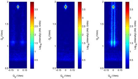
Figure 1. GISAXS images
taken during the growth of a diindenoperilene (DIP)
film at thicknesses of 0.5, 1.0 and 1.5 monolayers (left, middle, and right, respectively). The
diffuse scattering present in left and right images is due to the presence of
DIP molecular islands. Almost no diffuse scattering is present at 1.0 monolayer
of DIP, since the layer is completed and no islands are present. The
enhancement of intensity at Qz=1.05 nm-1 corresponds to the Yoneda
wing of the thin film. The intense peak around Qz=1.9
nm-1 is the specular reflection from the sample at the anti-Bragg point
of DIP standing phase.