Scanning x-ray submicron diffraction on 3D heteroepitaxial microcrystals
M. Meduňa1, C.V. Falub2,
D. Chrastina3, F. Isa3, A. Marzegalli4, T.
Kreiliger2, A. G. Taboada2, G. Isella3, L.
Miglio4, H. von Känel2
1Department of Condensed Matter Physics & CEITEC, Masaryk University, Kotlářská 2, 61137 Brno, Czech Republic
2Laboratory for Solid State Physics, ETH-Zürich, Schafmattstrasse 16, 8093 Zürich, Switzerland
3L-NESS, Department of Physics, Politecnico di Milano, via Anzani 42, 22100 Como, Italy
4L-NESS, Department of Materials Science, Universita di Milano-Bicocca, via Cozzi 53, 20126 Milano, Italy
mjme@physics.muni.cz
Monolithic integration of other semiconductor materials onto silicon substrates is expected to extend Si-based technology towards new optical and electrical functionalities inaccessible by the mere dimensional scaling predicted by Moore’s Law. Unless wafer bonding techniques are used, such integration of dissimilar materials necessarily involves hetero-epitaxial growth. However, the growth of epitaxial layers on a single crystal substrate usually results in undesired defect formation above a certain critical thickness, if the corresponding crystal lattices exhibit a poor match of lattice parameters or thermal expansion coefficients.
Recent achievements demonstrate that extremely thick Ge-layers with exceptional crystalline quality can be monolithically integrated onto a Si CMOS platform despite the large lattice and thermal mismatches. Dislocations, layer cracking and wafer bowing could all be eliminated by a novel mask-less deposition process wherein high-quality Ge towers are epitaxially grown by LEPECVD technique on micron size structures with high aspect ratios machined into a clean, patterned Si-wafer [1,2].
In this work we present x-ray diffraction structural study of various types of Ge crystals epitaxially grown in shape of elongated pillars on prepatterned Si substrates (Fig. 1). The Ge crystals height ranged from 1 to 8 mm and different patterns were explored. The typical area of pillars was ~ 2´2 mm2 separated by 1 mm wide trenches.
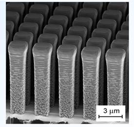
Figure 1. SEM image of epitaxial grown Ge crystals on etched 8 mm Si pillars shows 1.2 mm high crystals having pillar period 3 mm and 1 mm large trench.
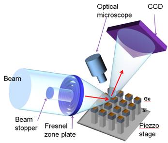
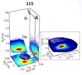
The aim of the structural investigation of the Ge pillars was to determine crystal lattice tilt and strain as from whole pillars as locally within the pillar. Thus XRD measurements in coplanar geometry around the symmetric (004), and the asymmetric (115) reflections were performed using a focused beam. The experiment was realized at ESRF, Grenoble, at the ID01 beamline, which is equipped with a Fresnel zone plate, so that the final beam spot size was ~ 500´300 nm (Fig. 2). Such condition allowed us to map the diffracted intensity across the individual pillars and to obtain (x,y) position map of diffracted intensity. Using a 2D pixel detector, 3-dimensional reciprocal space maps (RSMs) were constructed for each (x,y) position of the x-ray beam on the sample (Fig. 3).
|
|
|
|
Figure 2. Experimental setup of scanning nanodiffraction experiment. |
Figure 3. Example of 3D reciprocal space map recorded in the middle of the 3.1 um pillar showing detailed cut through Ge diffraction peak. |
The analysis of 3D RSMs recorded at 2D surface mesh
allowed us to obtain the (x,y) map of lattice tilt,
strain and relaxation within Ge pillars. The results
show that the crystal planes close to Ge/Si interface
are bent due to elastic relaxation of thermal strain which develops during
cooling from the growth temperature. By scanning diffraction technique we were
able to distinguish between lattice bending and tilts of the whole crystals.
The lattice bending was in very good agreement with the finite element
calculations [3,4].
References
1. C.V. Falub, H. von Känel, F. Isa, R. Bergamaschini, A. Marzegalli, D. Chrastina, G. Isella, E. Müller, P. Niedermann, L. Miglio, Science, 335, (2012), 1330.
2. H. von Känel and L. Miglio, international patent application WO/2011/135432.
3. C. V. Falub, T. Kreiliger, A. G. Taboada, F. Isa, D. Chrastina, G. Isella, E. Mueller, M. Meduňa, R. Bergamaschini, A. Marzegalli, E. Bonera, F. Pezzoli, L. Miglio, P. Niedermann, A. Neels, A. Pezous, R. Kaufmann, A. Dommann and H. von Känel, International Semiconductor Conference (CAS) 2, (2012), 45.
4. C. V. Falub, M. Meduňa, D. Chrastina, F.
Isa, A. Marzegalli, T. Kreiliger, A.G. Taboada, G. Isella, L. Miglio, A.
Dommann, and H. von Känel, Scientific Reports 3 (2013), 2276.
Acknowledgements.
We acknowledge program funding Nano-Tera through project NEXRAY, the staff of ID01beamline at ESRF, project Research4Industry (CZ.1.07/2.4.00/17.0006) and the FIRST Center for Micro- and Nanoscience of ETH Zürich for making available its infrastructure.