Structural analysis of GaAs/Si nanowires
P. Klang1, H. Detz1, A. M. Andrews1, D. Kriegner2,
J. Stangl2, G. Bauer2,
A. Lugstein3,
W. Schrenk3, G. Strasser1,3
1Institute for Solid State Electronic, TU-Wien, Vienna, Austria
2Institute of Semiconductor Physics, Linz University, Linz, Austria
3Center for Micro- and Nanostructures, TU-Wien, Vienna, Austria
pavel.klang@tuwien.ac.at
Semiconductor nanowires have been intensively studied as a potential structure to merge Si-based technology with the field of III-V optoelectronics. The structural properties of ensembles of GaAs nanowires grown on Si nanowire templates are studied non-destructively by X-ray diffraction to determine epitaxial orientation, crystalline quality, and crystal structure.
The GaAs nanowires were grown using molecular beam epitaxy on Si nanowire templates. The templates were prepared by the vapor-liquid-solid growth mechanism in a low pressure chemical vapor deposition reactor [1]. The GaAs nanowhiskers formed tree-like structures with a 6-fold radial symmetry (Fig. 1) on the side facets of the Si nanowires trunks [2].
We identified both wurtzite and zinc-blend structure of GaAs in the samples from measured reciprocal space maps with a large Qz range. Additional to the maps, we investigate pole figures to find the epitaxial relationship between GaAs and Si crystal structures. The peak positions in the pole figures for Si 111 and GaAs 111 diffraction are the same, therefore we can conclude that the GaAs nanowires are grown hetero-epitaxially on Si nanowires. The six-fold symmetry of the nanowire trees is observed also in the pole figure measurements. In this measurement for the GaAs 111 diffraction, we should obtain only four peaks corresponding to the <111> directions for pure zinc-blend GaAs. In the measured pole figures, there are additional peaks not expected for bulk GaAs. These peaks can be explained by considering the effects of twin defects in {111} planes in the Si and GaAs nanowires (Fig. 2). Due to the high intensity of these additional peaks a significant fraction of the Si and GaAs nanowires contain twin defects. This is in a good agreement with high resolution transmission electron microscopy analysis.
![]()
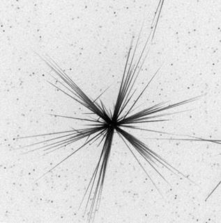
Figure 1. SEM picture of GaAs nanowhiskers on Si nanowire forming tree-like structure with a 6-fold symmetry.
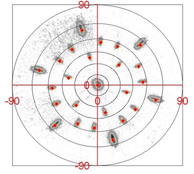
Figure 2. Measured X-ray pole figure for GaAs 111 diffraction and calculated <111> peak positions taking account twin defects in {111} planes.
We recorded three grazing incidence diffraction reciprocal space maps to determine the wurtzite content of the nanowires. We chose the cubic (-1-11) and (311) reflections and the cubic/hexagonal (-220)/(-1-120) reflection because they are accessible in the grazing incidence geometry. We compared the measured integrated intensity with the theoretical reflection strength of GaAs for these reflections. The high intensity of the wurtzite allowed reflection implies 80-90% wurtzite in the sample, but this also includes the GaAs that did not incorporate into the nanowires.
Hetero-epitaxially grown GaAs nanowhiskers on Si nanowires were characterize non-destructively by X-ray diffraction. We were able to identify the effect of twin defects in {111} planes of the nanowires in the measurement. The planar defects explain the additional peaks and their positions in the pole figure diagrams. We include the twins to the model of GaAs nanowires grown along <111> or <0002> direction on the {112} side facets of the [111] Si nanowires trunks. Using grazing incidence diffraction, we measured the wurtzite content of the GaAs nanowires.
References
1. A. Lugstein, A.M. Andrews, M. Steinmair, Y. Hyun,
E. Bertagnolli, M. Weil, P. Ponratz, M. Schramböck, T. Roch, G. Strasser, Nanotechnology,
18, (2007), 355306
2. H. Detz, P. Klang, A.M. Andrews, A. Lustein, M.
Steinmair, Y.J. Hyun, E. Bertagnolli, W. Schrenk, G. Strasser, Journal of Crystal Growth, 311, (2009), 1859
Acknowledgements.
The authors would like to gratefully acknowledge the support of the Austrian SFB project IR-ON and Society for Micro- and Nanoelectronics (GMe).