X-ray laboratory with rotating anode of the
Consortium MULTIDISC of SAS – capabilities of the diffractometer Bruker D8
DISCOVER
1Institute
of Electrical Engineering, SAS, Dúbravská cesta 9, 841 04,
2Institute
of Physics, SAS, Dúbravská cesta 9, 845 11,
elekdobr@savba.sk
Abstract
A brief history of an X-ray laboratory of Consortium MULTIDISC founded by several institutes of the Slovak Academy of Sciences is outlined. The diffractometer Bruker D8 DISCOVER with rotating anode located in the laboratory is described. A selection of representative results is introduced to show a wide scope of applications of the diffractometer covering different types of structural analyses.
Introduction
The history of our X-ray laboratory with
rotating anode started in 2005 when the Consortium for multidisciplinary
research of materials MULTIDISC was established. At present, four institutes of
the Slovak Academy of Sciences – Institute of Physics (IP), Institute of
Electrical Engineering (
Instrumentation
The X-ray tube with rotating Cu anode (line
focus 10 x 0.5 mm) is designed for the maximum power of 18 kW,
but in practice 12 kW is used for all measurements. The Göbel mirror
attached to the body of the tube delivers a quasi-parallel primary beam
1.2 mm wide and with a divergence of ~ 0.03°. This solution is suited for thin film analyses but excludes the
possibility to change the set-up to Bragg-Brentano geometry. The automatic
absorber (4 values of absorption factor) enables to measure the intensities
over 9 orders of magnitude. The central Eulerian cradle allows to perform
texture and stress analysis. A precise sample alignment is supported by motorized
sample stage (X, Y in-plane shifts by +/- 40 mm, Z shift ranges from -1 to +2 mm).
The radiation is collected by a NaI(Tl) scintillation point detector. The diffractometer
design is modular with a 4‑bounce Bartels monochromator for the primary
beam with two Ge(022) channel-cut crystals, a pathfinder for the diffracted
beam switching automatically between a slit and a 3-bounce Ge(022) channel-cut
crystal analyzer, two Soller slits (0.12° and 0.35°
divergence) for coplanar grazing incidence diffraction, a LiF monochromator for
suppression of sample fluorescence and a knife-edge collimator for reflectivity
measurements. Polycrystalline diffraction in symmetrical (SymD) and grazing
incidence (
Operation and exploitation of the laboratory
The operating staff of the laboratory has
only two members, E. Dobročka (
As mentioned above, the primary task of the laboratory is analyses of thin films prepared by various deposition technologies. This requirement affected considerably the basic set-up and the selection of the optical elements of the diffractometer. As a consequence, Bragg-Brentano geometry is impossible due to the fixed Göbel mirror, aggravating thus investigations of bulk polycrystalline materials. This can be seen in Table 1 where the operating hours-per-year of the diffractometer are shown for all four institutes. Two institutes clearly dominate in the exploitation of the diffractometer which is in agreement with their research field focused on thin film technologies. Nevertheless, the high power of the X-ray tube partly mitigates absence of the benefits of Bragg-Brentano geometry for polycrystalline samples and renders the diffractometer very useful also for IACH and IMMM. A division across particular Departments of the main methods used is the following:
Department of Multilayers and Nanostructures (IP): XRR, diffuse
scattering,
Department of Metal Physics (IP): SymD,
Department of Thin Oxide Films (
Department of Optoelectronics (
Department of Cryoelectronics (
Department of Superconductor Physics (
Department of Semiconductor Technology and Diagnostics (
Department of Ceramics (IACH): SymD,
Department of Hydrosilicates (IACH): SymD.
Department of Properties of Materials & Structures (IMMM): SymD,
Department of Microstructure of Surfaces &
Interfaces (IMMM): SymD,
Table 1. Exploitation
of the diffractometer Bruker D8 DISCOVER
|
|
2006 |
2007 |
2008 |
2009 |
||||
|
Institute |
hours |
% |
hours |
% |
hours |
% |
hours |
% |
|
IP |
849 |
59 |
293 |
23 |
1101 |
57 |
738 |
44 |
|
|
542 |
38 |
831 |
64 |
451 |
23 |
639 |
38 |
|
IACH |
20 |
1 |
71 |
6 |
160 |
8 |
130 |
8 |
|
IMMM |
31 |
2 |
91 |
7 |
220 |
12 |
167 |
10 |
|
Total in year |
1442 |
100 |
1286 |
100 |
1932 |
100 |
1674 |
100 |
Examples of results
The list of Departments using the services of our X-ray laboratory proves that its research scope is wide. During the whole operation period of the diffractometer, a vast number of results from various scientific fields was obtained. In the following we present just a few examples of measurements that we consider to be either interesting due to surprising results or illustrative to show the capabilities and flexibility of the diffractometer. A comprehensive analysis and interpretation of the results is out of the scope of this contribution and was (or will be) published elsewhere.
Texture analysis of YBaCuO superconductor films grown on GaN
Active and
passive elements based on
The YBaCuO
HTS thin films on c-oriented GaN/sapphire substrates were grown at the
Department of Cryoelectronics of
The texture
of both types of samples was analyzed in our X-ray laboratory. The aim of the
analysis was to determine the degree of preferred orientation of the YBaCuO
blocks with respect to the sample surface normal and to find a possible effect
of the MgO buffer layer on the structural quality of the HTS films. In
Figs. 1 and 2, the (103) pole figures of YBaCuO films grown without and
with the MgO buffer layer, respectively, are compared. For the sake of
simplicity, here we do not distinguish between the (103) and (013) planes of
the orthorhombic YBaCuO lattice due to their similar interplanar distances. The
angle between these planes and the c-axis of the YBaCuO lattice is ~45°.
|
|
|
|
Figure 2. Pole figure (103) of YBaCuO layer grown directly on GaN/sapphire substrate. The range of angle χ is 30 – 60°. |
Figure 3. Pole figure (103) of YBaCuO layer grown on MgO buffer layer deposited on GaN/sapphire substrate. The range of angle χ is 40 – 50°. |
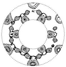
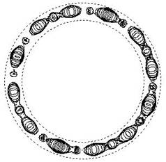
In both figures 12 strong and 12 weak maxima can be recognized. While in the sample with MgO buffer layer all maxima are localized around the χ angle ~45°, in the sample without buffer layer the strongest maxima are at wrong positions indicating that the most of the crystallites have their c-axis inclined with respect to the substrate normal. The in-plane symmetry of both pole figures reflects the combined three-fold symmetry of the (001) GaN or (111) MgO surface and the four-fold one (considering the YBaCuO lattice to be almost tetragonal) of the YBaCuO crystallites. We can conclude that the MgO buffer layer improves the structural quality as well as the superconducting properties of the HTS films grown on GaN/sapphire substrates.
Precipitation
of MnAs in InAs epitaxial films
The incorporation
of manganese in InAs semiconductor can provide a spintronic material. If the
content of Mn exceeds a certain value, precipitation of MnAs phase within the
InAs epitaxial layer occurs. As the MnAs particles are hexagonal, interesting
orientation relationship between the MnAs lattice and the cubic matrix can be
expected. It is assumed that the c-axis of MnAs lattice is perpendicular to the
{111} planes of the InAs matrix. However, the diffraction (102) of MnAs is
usually visible in the standard 2θ/θ diffraction patterns indicating
that precipitates of different orientations are also present in the InAs layer.
The Mn-doped
InAs epitaxial layers grown on (001) GaAs substrates were prepared at the
Department of Optoelectronics of
|
|
|
|
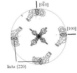
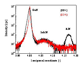
Figure 3. Pole figure (102) of MnAs precipitates in In(Mn)As epitaxial layer. The range of angle χ is 0 – 50°. |
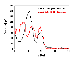
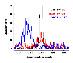
Figure 4. χ scans of MnAs (102) diffraction toward two perpendicular directions [110] and [1-10] of the InAs layer lattice. |
Spatially resolved diffraction
In the past years a number of studies have been published on various aspects of the reactions between Sn-Ag, Sn-Cu and Sn-Ag-Cu alloys and various substrates. Reaction between Sn in these molten solders and Cu substrate at the Cu/solder interface results in the formation of Cu6Sn5 and Cu3Sn phases. At the Department of Microstructure of Surfaces & Interfaces of IMMM the influence of indium addition to SnAgCu solder on the microstructure of the interface between solder and cupper substrate was studied [3]. Our X-ray laboratory was involved in this analysis with the aim to reveal the spatial distribution of the phases with respect to the solder/Cu interface.
Figure 5. 3D view of a set of detector scans recorded at 10 different positions across the SnAgCuIn solder/Cu interface. Graphical output of the evaluation software EVA (Bruker)
In order to solve this problem, a
modification of the grazing incidence set-up was employed. The fixed incidence
angle ensured that the width of the irradiated area and the penetration depth
did not vary during the measurement and the analysis of the results was
simplified. However in contrast to conventional
Testing of V-shaped GeSi monochromators
In standard (220) X-ray beam compressing monochromators for Cu Kα radiation, a total beam compression up to the factor of 10 can be achieved by V-shaped monochromators prepared from a pure germanium single crystal. A higher factor of compression is possible using larger angles of asymmetry. However, the total intensity of the beam is considerably decreased due to the refraction effect. One possibility to overcome this drawback is to use graded GeSi single crystal instead of a pure one.
At the Department of Semiconductor
Technology and Diagnostics of
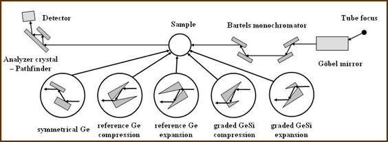
Figure 6. Scheme of the high-resolution set-up. In the circles in lower part of the figure, the top views of the samples and the beam traces are shown for 5 different types of measurement.
On the basis of our measurements we concluded that the intensity loss due to the refraction effect, that takes place in the case of V-channel monochromators, can be compensated by the composition grading of the parent single crystal of the monochromator. In the case of graded GeSi monochromator with the asymmetry factor of 21, more than three times higher intensity was obtained in comparison with the reference monochromator having the same design [4].
HRD – linear scans in reciprocal space
The PC
control of the up to date diffractometers enables to perform linear scans in
reciprocal space that can be useful for the analysis of lattice mismatch of
epitaxial films. For high quality semiconductor compounds the lattice mismatch
is of the order of 0.1 % or less and the asymmetric diffractions can
easily be measured by standard angular scans. However, in some advanced
technologies epitaxial layers with lattice mismatch exceeding 1 % are often
used. In this case, the layer diffractions are too far from the substrate ones
and the angular scans are inapplicable for measuring the asymmetric
diffractions. Instead of performing a complete map of an area in the reciprocal
space, linear scans can be used to find the layer peaks.
At the
Department of Thin Oxide Films of
|
|
|
|
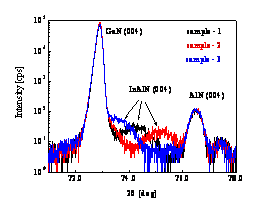
Figure 7. Symmetrical 2θ/ω scans of GaN (004) diffraction for three samples with different In content. |
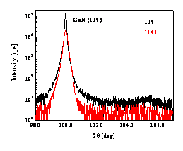
Figure 8. Asymmetrical 2θ/ω scans of GaN (114) diffractions of sample – 2. 114– is grazing incidence geometry, 114+ is grazing exit geometry. |
|
|
|
|
Figure 9. Linear l scans through (004) and (114) points of GaN reciprocal lattice. |
Figure 10. Linear h scans for three different values of l coordinate at the (114) point of GaN reciprocal lattice. |
Firstly, the l coordinate of the layer peaks are read-out from the l scan across the (004) point (Fig. 9). The h scans performed with these values of the l coordinate at the asymmetrical point (114) revealed a perfect lateral match between GaN and InAlN and the shift of the AlN peak by 2.5 % with respect to GaN. All curves except for the h scan at l = 4.00 (Fig. 10) were measured without the analyzer crystal.
Acknowledgement
The work described was supported by
SAV-FM-EHP-2008-01-01 project financed within EEA mechanism and
References
1. Š.
Chromik, P. Gierlowski, M. Španková, E. Dobročka, I. Vávra, V. Štrbík, T.
Lalinský, M. Sojková, J. Liday, P. Vogrinčič, J. P. Espinos, Appl. Surf.
Science, in press.
2. J. Novák,
3. P. Šebo, Z. Moser, P. Švec, D. Janičkovič, E. Dobročka, W. Gasior, J. Pstrus, J. Alloys and Compounds, 480, (2009), 409-415.
4. D. Korytár, C. Ferrari, P. Mikulík, P. Vagovič, E. Dobročka, V. Áč, P. Konopka, A. Erko, N. Abrosimov, J.Appl. Cryst., 43, (2010), 176-178.
5. http://www.morganproject.eu/