Electron diffraction, elemental and image analysis of nanocrystals
M. Šlouf1,
E. Pavlová1, J. Hromádková1, D. Králova1, V.
Tyrpekl2
1Institute of Macromolecular Chemistry of the Academy of Sciences of the Czech Republic, v.v.i.,
Heyrovskeho namesti 2, 16206 Praha 6, Czech Republic
2Institute of Inorganic Chemistry fo the Academy of Sciences of the Czech Republic, v.v.i.,
250 68 Husinec-Rez 1001, Czech Republic
slouf@imc.cas.cz
Keywords: electron diffraction, energy dispersive analysis of X-rays, nanocrystals
Abstract
Transmission electron microscope (TEM) can operate in four main modes: bright field (BF), dark field (DF), electron diffraction (ED) and energy-dispersive analysis of X-rays (EDX). A TEM microscope working in all above mentioned modes (BF, DF, ED and EDX) is usually called the analytical electron microscope. It is a powerful tool for study of nanocrystals, which are invisible in light microscopes and do not diffract X-rays sufficiently. TEM/BF in combination with image analysis yields a quantitative description of nanocrystal shapes. TEM/EDX gives elemental composition of nanoparticles. TEM/ED in combination with crystallographic databases identifies known crystal structures. TEM/DF may differentiate monocrystals from twins.
Introduction
Resolution of modern TEM microscopes is well bellow 1 nm, which makes them suitable tools for study of nanoparticles and nanostructures in bulk materials. Both nanoparticles and nanostructures cover broad range of applications in materials science (inorganic nanoparticles, nanolayers, defects in metals and alloys), polymer science (synthetic polymer nanocomposites, block copolymers, polymer micelles) and biology (morphology of cells and viruses). This contribution is focused on analysis of nanoparticles, namely nanocrystals.
A standard modern transmission electron microscope (TEM) operates in three modes: bright field (BF), dark field (DF), and electron diffraction (ED, SAED). In TEM/BF we detect transmitted electrons and receive a "standard" TEM micrograph: a direct image, in which the dark areas appear due to diffraction and/or absorption contrast. In TEM/DF we detect (a selected portion of) scattered/diffracted electrons and obtain a direct image with "inverted" contrast. In TEM/ED we detect scattered/diffracted electrons in a different way and obtain electron diffraction pattern, which is analogous to X-ray and neutron diffraction patterns.
As an extra option, TEM microscope can be equipped with a EDX detector and work in mode of energy dispersive analysis of X-rays (EDX, EDS). In such a case we can detect characteristic X-rays and, as a result, perform elemental analysis in nanoscale. A TEM microscope equipped with the four basic modes (BF, DF, ED, EDX) is usually called the analytical electron microscope.
It is a matter of course that there are also more advanced and/or special modes of TEM, such as high-resolution transmission electron microscopy (HRTEM), convergent beam electron diffraction (CBED), scanning transmission electron microscopy (STEM), energy-filtered transmission electron microscopy (EFTEM), cryo transmission electron microscopy (cryoTEM) - just to name a few. Nevertheless, this contribution concentrates on the explanation of four basic modes (BF, DF, ED, EDX) and their application on study of nanocrystal shapes, elemental composition and crystal structure.
Selected
theory
A modern TEM microscope is a complex optical device. Complete description of electron paths in the microscope requires high-level mathematics and physics. Nevertheless, the key features of the microscope, important from user's point of view, can be explained in a relatively simple way, as illustrated below.
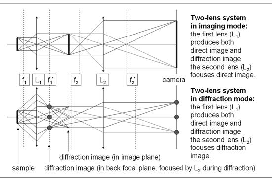
TEM microscope yields both direct and diffraction images. Moreover, in modern microscopes the switch between direct and diffraction consists in pressing a single button. The basic explanation how this is possible is surprisingly simple, being based just on elements of ray optics (Fig. 1). Similar ray diagrams can be drawn for the whole TEM microscope; they can explain not only the difference between imaging and diffraction mode, but also the difference between bright-field and dark-field, selected-area electron diffraction (SAED, traditional technique) and apertureless diffraction (ED, recent technique) etc.
|
|
|
|
Figure 1. Imaging and diffraction mode in TEM. |
Figure 2. Single crystal diffraction in XRD and ED. |
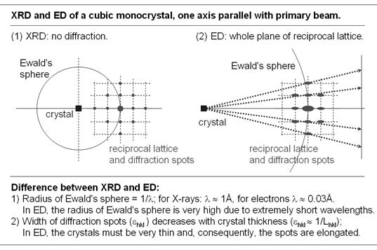
For single crystal X-ray diffraction, we need to use four-circle diffractometers and collect diffractions step-by-step, using either point detectors or 2D-detectors, such as CCD cameras, image plates of films. In a TEM microscope, we can see the whole plane of reciprocal lattice in one image. The basic explanation is again relatively straightforward, employing just Ewald's construction, calculation of electron wavelength and one simple formula from Fourier theory (Fig. 2).
Selected experimental
results
Important advantage of TEM investigations is the fact that we can apply more methods in the same sample and obtain complete information concerning its morphology, composition and crystal structure. Figure 3 shows CeO2 nanocubes, which were synthesized in order to be used as a microscopic marker, distinguishable from widely used spherical nanoparticles. Cubic shape of CeO2 nanocrystals was apparent from TEM/BF (Fig. 3a), more detailed analysis of shapes could be performed with image analysis software [1]. Monocrystalline nature of CeO2 nanocubes was indicated by TEM/DF (Fig. 3b), as the selected diffractions come from the whole nanocrystals and not just their parts. Diffraction pattern of the observed CeO2 nanocubes was readily obtained by means of electron diffraction (inset in Fig. 3c); ED pattern was further processed [2] and compared with calculated with calculated X-ray diffraction [3], which confirmed the CeO2 crystal structure (Fig. 3c). EDX analysis of CeO2 nanocubes (Fig. 3d) yielded peaks corresponding to the investigated sample (Ce, O), but also a signal from carbon-coated copper grid, on which the nanocrystals were deposited (C, Cu), and signal from impurities such as dust and oil from the nanoparticle synthesis (C, Si, O).
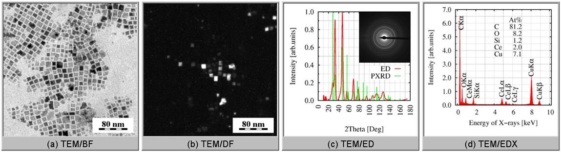
Figure 3. CeO2 nanocubes in TEM: (a) bright field, (b) dark field, (c) electron diffraction, (d) EDX spectrum.
Conclusion
This contribution briefly describes principle and application of analytical transmission electron microscope, i.e. a TEM microscope, which works in bright field (BF), dark field (DF), electron diffraction (ED, SAED) and X-ray microanalysis (EDX, EDS) modes. Such a microscope can be used, among other things, for analysis of nanocrystals, which are too small and/or available in too small amounts for X-ray diffractometers.
References
1. Program ProcessDiffraction: J. L. Lábár, Microscopy and Analysis, 75 (2002) 9-11.
2. Program PowderCell: http://www.ccp14.ac.uk/tutorial/powdcell/index.html.
3. Program NIS Elements: http://www.lim.cz.
Acknowledgements.
Financial support through grants KAN200520704 a GACR 203/07/0717 is gratefully acknowledged.