X-ray Characterization of GaAs Nanowires Grown on Si Nanowires
P. Klang1, A.M. Andrews1,2, H. Detz1, A.
Lugstein2, W. Schrenk1, G. Strasser1,3
1Center
for Micro- and Nanostructures, TU-Wien, Floragasse 7,
2Institute
for
3Departments
of Electrical Engineering and Physics, The
klang@fke.tuwien.ac.at
Combining the benefits of silicon with III-V semiconductors is a goal to producing novel structures for electronic and optoelectronic applications. The Si nanowire templates were grown epitaxially on Si (111) substrates using the vapor-liquid-solid growth mechanism in a low-pressure chemical vapor deposition reactor. A 2 nm thick gold layer was previously sputtered on the substrate surface to serves as a catalyst for the silicon nanowire growth. GaAs nanowhiskers were grown on the silicon nanowire trunks in a solid-source molecular beam epitaxy system. The GaAs nanowhiskers formed tree-like structures with a 6-fold radial symmetry on the {112} side facets of the [100] Si nanowires trunks [1]. We present the x-ray diffraction study of the crystal structure of this material system.
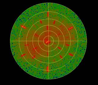
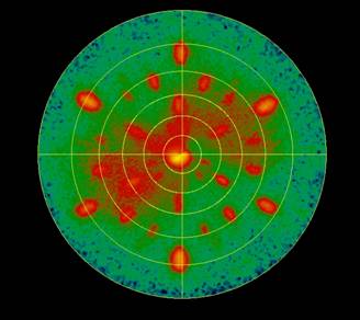
Figure 1. Pole figures for Si 111 and GaAs 111 (0002) diffraction.
The high-resolution x-ray diffraction measurements were performed to study the crystal properties of the GaAs nanowhiskers grown on the Si nanowire trunks. From the measured x-ray diffraction spectra we identified Si, wurtzite and zinc-blend GaAs, Au and AuGa diffraction peaks [2]. Additional to the reciprocal space maps, we measured the pole figures for the Si 111 and GaAs 111 diffraction conditions (equivalent to wurtzite 0002 diffractions) to find the relationship between Si and GaAs crystal structures. The peak positions in the pole figure for Si 111 diffraction are in a very good agreement with the peaks in the pole diagram for GaAs 111 diffraction (see Figure 1) and, therefore, we can conclude the GaAs nanowhiskers were grown hetero-epitaxially on the sidewalls of silicon nanowires.
For better understanding of crystal
properties of GaAs nanowhiskers, we investigate the growth of the GaAs
nanowires on planar Si (112) wafers with various pre-growth surface treatments. We
removed the native silicon oxide using buffered hydrofluoric acid (HF) from one
half of the Si (112) wafer. A 2 nm thick sputtered Au layer was deposited
on the surface as a catalyst. The final step was an additional HF dip to obtain
4 different zones on the sample. At the end, we grew GaAs with the equivalent layer
thickness of 200 nm in our molecular beam epitaxy system. The 4 different
zones were visible on the surface after the growth. High density oriented
nanowires were observed only on the part of the sample which was exposed to HF
only after the Au layer deposition. The scanning electron microscopy (SEM)
image of the cleave edge of this part of the sample is shown in the Figure 2.
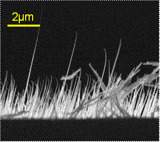
Figure 2. SEM image of the GaAs nanowires grown on Si (112) substrate tilted by 19.65°.
We observed ordered GaAs nanowires on Si (112) substrate. From the SEM image of the cleaved edge we can see that these nanowires are tilted under an angle of 19.65° from the substrate normal. This tilt corresponds to the angle between [112] and [111] direction. High resolution TEM analysis confirmed that the GaAs [0001] nanowires were grown in the wurtzite crystal structure along the Si [111] direction as we expected from XRD and SEM.
The pole figures of Si 111 and GaAs 111 diffraction confirm the hetero-epitaxial growth of the GaAs nanowhiskers on silicon nanowire trunks. Based on the analysis of GaAs nanowires grown on Si (112) substrates we can conclude the GaAs nanowhiskers are grown on the {112} facets of the Si nanowire trunks in the Si [111] directions. We also confirmed the wurtzite structure of the GaAs nanowhiskers with the [0001] growth direction.
References
1. A. Lugstein, A.M. Andrews, M. Steinmair,
Y. Hyun, E. Bertagnolli, M. Weil, P. Ponratz, M. Schramböck, T. Roch, G.
Strasser, Nanotechnology, 18, (2007), 355306
2. H. Detz, P. Klang, A.M. Andrews, A.
Lustein, M. Steinmair, Y.J. Hyun, E. Bertagnolli, W. Schrenk, G. Strasser,
Journal of Crystal Growth, 311, (2009), 1859