Towards limits of x-ray specular reflectivity
J. Jíša and M. Meduňa
Department of Condensed Matter Physics, Kotlářská, 611 37 Brno
janjisa@mail.muni.cz
In the last decades, thin film technologies found numerous applications in many physical, technological and industrial fields and are used in various procedures within research in microelectronics, optoelectronics, optics, biology and nanotechnology. The production of semiconductor devices, integrated circuits, recordable media such as optical discs and hard-discs, or special coatings and filters on optical elements are based on thin film technology. The production of thin films requires determination of their properties, which are necessary to parameterize the designed structure of the device being processed. Thickness, density, material composition, crystalline structure, refractive index and interface roughness in individual layers of the structure are typical parameters investigated during the layer growth.
In order to characterize the layers, there are many techniques for investigation of thin film properties, usually based on the interference of electromagnetic radiation. These methods covering wavelengths from infrared optics up to x-rays have an advantage of non-destructive diagnostics. Optical reflection and ellipsometry are mostly used for thick layers with thicknesses of around 1 mm. On the contrary, x-ray specular reflectivity is much more sensitive to very thin layers down to 0.5 nm and roughness down to 0.1 nm [1,2]. A disadvantage of commonly used x-ray reflectometers is the upper limit of layer thicknesses (~100 nm), determined mainly by the lower resolution of x-ray optics used in the measurement setup for x-ray reflectivity.
In this work, we investigate the thickness and roughness of thin films of photoresists produced by spin coating (centrifugal casting) on silicon wafers. This procedure, which is standardly used during the production of integrated circuits in industry, is performed inside the clean room laboratory at the Department of condensed matter physics.
The spin coating method consists of depositing a small amount of liquid photoresist on a silicon wafer and subsequent spinning of the wafer up to 1000-6000 rotations per minute. A very thin, almost homogeneous and rapidly drying up photoresist layer is formed due to centrifugal forces and surface tension of the fluid. The silicon wafer with the layer is then baked at 90 - 120 °C for 3 - 5 minutes. Such a layer proceeds into the next technological step like litography and etching, where only the illuminated or un-illuminated areas are removed, according to negative or positive photoresist used. The sequences of deposition of materials with various properties (metalization, doping, etc.) are repeated combining negative or positive photoresists and other chemical procedures during the technological steps which consequently determine the structure of the designed semiconductor device. Thus the calibration of photoresist thicknesses is very important.
Determination of the thickness from x-ray specular reflectivity utilizes the interference of x-rays reflected and transmitted at the air-layer interface and the layer-substrate interface depending on the angle of incidence [3,4]. The method is commonly used for layers where the thickness is only about 2-200 times larger than the wavelength of the used radiation (very occasionally more than 1000 times). For CuKa wavelength, this gives a limit of hundreds of nm for the layer. Larger thickness can be hardly measured since the interference oscillations are suppressed by the resolution function of the monochromator, various interface roughnesses, absorption in the layer and statistical noise of the signal. In our experiment we measure layer thicknesses more than 10000 times larger than the wavelength using high-resolution diffractometer [3] and Fourier transform analysis [5,6].
|
|
|
|
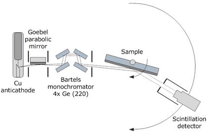
Figure 1. Schematic of
the experimental setup. |
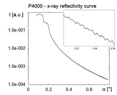
Figure 2. Measured x-ray
reflectivity curve with a detail of the weak oscillations. |
The investigated photoresist layers prepared by spin coating were first measured by optical reflection probe, which is a method also based on the interference principle, but works in the visible range of spectrum (300 - 1000 nm) and in perpendicular reflection. Thicknesses of these photoresist layers depend on the angular velocity of the spinning during the deposition and vary within the range of 1100 - 1800 nm for the positive photoresist and in the range 800 - 1000 nm for the negative one. Although these thicknesses are extremely large to be measured by standard x-ray reflectivity, we have performed x-ray specular reflectivity scans as well and obtained similar values as with the optical measurements.
The setup of the x-ray reflectivity
experiment, see Figure 1, was following: x-rays leave a Cu anticathode and
continue to a Göbel parabolic graded multilayer
mirror where the beam is collimated and monochromatized.
A further double crystal Ge 220 Bartels monochromator permits propagation of only the CuKa1 radiation and lowers the in-plane angular divergence
down to 0.003°. Slits before the sample limit the beam to dimensions 0.3 mm x 8
mm. Such highly collimated and monochromatic beam hits the sample at a small
angle of incidence in the range of several degrees. The reflected beam
propagates through the next 0.3 mm wide slit towards the scintillation
detector.
The
interference oscillations in x-ray specular reflectivity measurement were so
weak, see Figure 2, that it is very difficult to fit the reflectivity directly
by an appropriate model. Moreover, the oscillations are significantly smoothed
out by the resolution function of the monochromator.
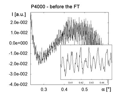
Thus we used a Fourier analysis similar to the one used by authors in Refs. [5,6]. In order to enhance the interference pattern, the
measured curve was divided by a theoretical reflection of smooth silicon
surface with a roughness of about 0.1-0.3 nm, see Figure 3. Parameters of this
theoretical curve such as roughness, index of refraction and absorption were fitted
manually in order to approximately match the measured curve. This operation
enhanced the oscillations and compensated the logarithmic decay in angular
space. The new curve was converted into reciprocal space (scattering vector
inside the substrate) – qz = 4p/l*(sin2(ai)-sin2(ac))1/2,
where ac is the critical angle for
photoresist. In the next step, we could simply determine the layer thicknesses
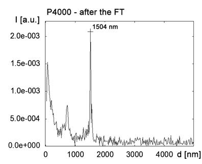
using the positions of peaks on the Fourier transformed curve, see Figure 4.
The distribution of peak positions corresponds to linear combinations of
possible thicknesses present within the photoresist coating deposited on the
silicon surface. The position of the most intensive peak corresponds to the
whole photoresist thickness.
|
|
|
|
Figure 3. Reflectivity
curve divided by the theoretical reflection of smooth Si surface. |
Figure 4. Fourier transform of the modified reflectivity curve in Figure 3. |
Using the high resolution diffractometer we have successfully measured photoresist
layers more than 1 mm thick by x-rays. The
thicknesses obtained by x-ray reflectivity correspond well to the ones obtained
by optical reflection and the maximum deviations are about 2.3 % for positive
photoresist layers and 8.5 % for negative ones.
References
1. P.Colombi, D.K.Agnihotri, V.E.Asadchikov, E.Bontempi, D.K.Bowen, C.H.Chang, L.E.Depero,
M.Farnworth, T.Fujimoto, A.Gibaud, M.Jergel, M.Krumrey, T.A.Lafford, A.Lamperti, T.Ma,
R.J.Matyi, M.Meduna, S.Milita, K.Sakurai, L.Shabelínikov, A.Ulyanenkov, A.Van der Lee and
C.Wiemer, J. Appl. Cryst., 41, (2008), 143
2. R.J.Matyi, L.E.Depero, E.Bontempi, P.Colombi, A.Gibaud, M.Jergel, M.Krumrey, T.A.Lafford,
A.Lamperti, M.Meduna, A.Van der Lee, C.Wiemer, Thin Solid Films, 516, (2008), 7962
3. V.Holý, U.Pietsch, T.Baumbach, High-resolution x-ray scattering from thin films and multilay,
Springer Tracts in Modern Physics, Vol.149, (Berlin: Springer) 1999, pp.120-135, 140
4. M.Tolan, X-Ray Scattering from Soft-Matter Thin Films, Springer Tracts in Modern Physics,
Vol.148, (Heidelberg: Springer) 1999
5. K. Sakurai, A. Aida, Jpn. J. Appl. Phys, 31, (1992), L113
6. K. Sakurai, M. Mizusawa, M. Ishii, Society of Japan 33, (2008), 523
Acknowledgements.
We would like to thank Václav Holý for regular thoughtful discussions and advices, Ondřej Caha for practical tips on handling an x-ray experiment, Petr Mikulík for providing the reflection probe measurement software and tutorials on the work in clean rooms and Milan Kučera for helping with depositions in the clean rooms. The work was supported by the projects 202/09/1013 of the Czech Science Foundation and MSM0021622410 of the Ministry of Education of the Czech Republic.