X-ray scattering on GaN thin films, Monte Carlo simulation
M. Barchuk1, V. Holý1, B. Miljevic2,
B. Krause2
1. Charles University in Prague, Faculty of Mathematics and Physics, Ke Karlovu 5, 12116 Praha 2, Czech Republic;
2. Forschungszentrum
Karlsruhe GmbH, Institute for Synchrotron Radiation,
Hermann-von-Helmholtz-Platz 1, D-76344 Eggenstein-Leopoldshafen, Germany.
Gallium nitride (GaN) is a most promising material for the base of photonic devices (LED and laser diodes, daylight visible full-color LED displays etc.). We investigate the defect structure of GaN epitaxial layers deposited by metalorganic vapor-phase deposition (MOVPE) on c-oriented sapphire substrates (Al2O3) covered by a thin AlN nucleation layer. The aim of our study is to determine the density of threading dislocations penetrating through the layer thickness towards free surface.
The large lattice mismatch between the GaN epitaxial layer and the applied substrate has a large influence upon the dislocation density increasing it to the order of 109 cm-2. The dislocation density can be reduced by in-situ deposition of a SiNX intermediate layer with sub-monolayer coverage [1]. This layer acts as a self-organized mask partially pinning the threading dislocations propagating from the substrate interface.
We used diffuse X-ray scattering in coplanar (0004) diffraction, the experiments were carried out at ANKA (Karlsruhe, Germany) on a 6-circle diffractometer at SCD beam-line
over a samples series with various nominal
thickness of the SiN pinning layer, the nominal thickness of GaN was between
1,8 to 2.4 mm, the sample description is given in Table
1. Depending on the thickness of the SiN
interlayer one could obtain different densities of threading dislocation that allowed
us to get a sufficient set of experimental data (reciprocal space maps - RSM),
radial and rocking curves, reflectivity measurements) and apply it for
comparison with simulated ones.
The approximate defect density in these samples was estimated by transmission electron microscopy (TEM – see Fig. 1) and from the etch pit density (Fig.2). Coincidence between these densities and the density following from our x-ray measurements is a proof of our theoretical approach for the defect description.
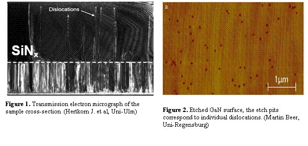
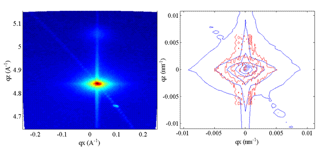
Figure 3 (a) presents an example of a
measured reciprocal-space distribution of x-ray intensity diffusely scattered
in symmetric diffraction 0004. Two maxima correspond to the AlN nucleation
layer (the upper weak maximum) and to the GaN epitaxial layer (the strong
maximum at ![]() Å-1).
Å-1).
Diffuse x-ray scattering from defects can
be described by conventional Krivoglaz theory [2]. In our case this approach is
not suitable because its numerical implementation for threading dislocations
contains very complicated integrals.
Therefore, we applied a Monte-Carlo simulation instead.
(a) (b)
Figure 3.
Experimental RSM of the sample S8134 in (0004) diffraction (a) and the comparison
measured (blue) and simulated (red) intensity distributions (b).
We generated random positions and types of threading dislocations, including a correlation in their positions, then we calculated the displacement field caused by the dislocations and the non-averaged amplitude of the scattered wave [3]. Performing a statistical average we obtained the scattered wave distribution in reciprocal space, i.e., the reciprocal space maps for different dislocation types (see characteristic examples in Fig. 4).
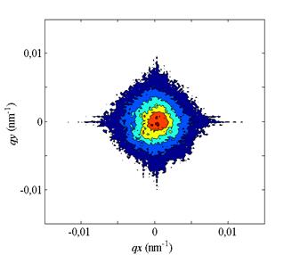
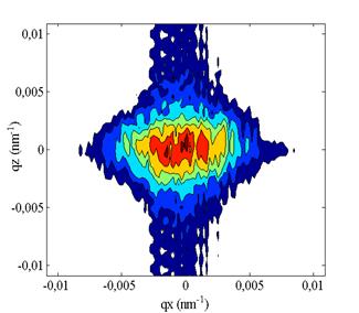
(a) (b)
Figure 4. Simulated RSMs for screw (a) and edge (b) threading dislocations in (0004) diffraction for the sample with the lowest dislocation density (S8134). The proportion between screw and edge dislocation densities is 1:10
From the set of experimental RSMs in symmetrical (0004) diffraction we could separate the contributions from pure screw and edge dislocations. In contrast to the screw threading dislocation, the edge ones appreciably contributed to intensity distribution in the qx-qz plane. Our main goal is to compare simulated and measured RSMs and their main cuts (Fig.3 (b)). Plotting both experimental and simulated cuts through the reciprocal-space intensity distribution along qx and qz axes in log-log representations (Fig.5) we are able to investigate the asymptotic behavior of the tails of the intensity profiles and to gain information about the prevailing dislocation type [4]. The estimated dislocation densities from our simulations are given in Table 1.
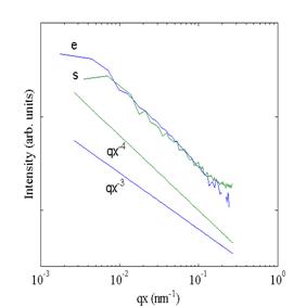
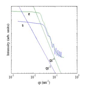
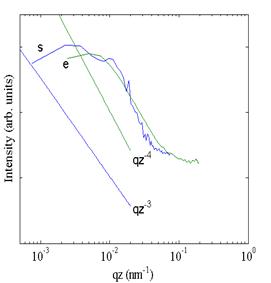
(a) (b) (c)
A detailed analysis demonstrates that the Monte-Carlo method can be used for the calculation of diffuse scattering from dislocations in epitaxial layers. For GaN layers in particular, this analysis makes it possible to determine the densities of individual types of dislocations.
|
Name of the sample |
SiNx deposition time, [s] |
Dislocation density (EPD), *108
[cm-2] |
Screw dislocation density from
simulations, *108 [cm-2] |
Edge dislocation density from
simulations, *108 [cm-2] |
Total dislocation density from
simulations, *108 [cm-2] |
|
S8134 |
180 |
2.6 |
0.3±0.1 |
2.7±1.1 |
3±1.2 |
|
S8135 |
150 |
4.8 |
- |
- |
5.0±1.5 |
|
S8136 |
120 |
7.6 |
- |
- |
7.5±2.2 |
|
S8071 |
0 |
20 |
2±0.6 |
21.5±6 |
23.5±6.5 |
Table 1.
The sample parameters
1. Hertkorn J. et al., J.
Crystal Growth 308, 30-36 (2007).
2. M.A. Krivoglaz, X-Ray
and Neutron Diffraction in Nonideal Crystals, Mater. Sci. Eng., A 49 (2001);
3. S.J. Shaibani and P.M. Hazzledine, Phyl. Magazine A, 1981, Vol. 44, No.3, 657-665.
4. V.M. Kaganer, O. Brandt, A. Trampert and K.H. Ploog, Phys. Rev. B 72, 045423 (2005).