Materials
Science Beamline at synchrotron ELETTRA, Trieste
M. Vondráček1, V. Cháb1, V. Matolín2, K.
C. Prince3
1Institute of Physics of the ASCR, v. v. i., Cukrovarnická 10, CZ-162 00 Praha 6, Czech Republic
2Charles University, Department of
Surface and Plasma Science, V Holešovičkách 2,
CZ-180 00 Praha 8, Czech Republic
3Sincrotrone Trieste S.C.p.A, Strada
Statale 14 - km 163,5 in AREA Science Park,
34012
Basovizza, Trieste, Italy
Keywords: Materials Science Beamline,
synchrotron, ELETTRA, photoemission spectroscopy
Introduction
Materials
Science Beamline at ELETTRA, Sincrotrone Trieste is probably the most complex
device used in synchrotrons, which was proposed, designed and manufactured
mainly by Czech companies and institutes and financed from European and Czech funds.
In the present time it is operated in close cooperation of three partners - Institute
of Physics of the ASCR, Charles University and Sincrotrone Trieste by the international
team with Czech participation. This 10 years long experience with construction,
operation, maintenance and never-ending improvement of MSB would be useful for
currently proposed ambitious project of Central European Synchrotron Laboratory
(CESLAB) in Brno.
ELETTRA
Synchrotron
ELETTRA was proposed as a soft X-ray complement of ESRF Grenoble in 80's. A
decision to build the two 3rd generation synchrotron facilities was
taken in 1986 and construction of ELETTRA began in 1991, reaching commissioning
in 1993. In contrast to older facilities, 3rd generation sources are
dedicated for synchrotron radiation not only from bending magnets, but also
from many of insertion devices (undulators, wigglers). They have low emittance
and then small beam size. ELETTRA storage ring with a circumference 259 m has
double bend achromate structure with 24 bending magnets and 11 long straight
sections dedicated for insertion devices [1]. Energy of circulating electrons
was originally proposed to 1.5 GeV with full energy injection from linac, but
early it was increased to 2.0 GeV with injection at 1.0 GeV. Later, the new
mode with 2.4 GeV energy was introduced (25% of user time). The latest
development represents a new full energy injection device consisting of 100 MeV
linac with a 2.4 GeV booster. Abandoned old linac will be rebuilt and become
the core of the FERMI@elettra 4th generation light source (free
electron laser).
Materials
Science Beamline
History
The idea to
build relatively simple and cheap beamline using bending magnet radiation with
photon energy in the range 20-1000 eV for the wide range of application in
materials science jointed together people from many institutions leaded by
Institute of Physics in Prague. Materials Science Beamline was proposed for the
first time as Italian-Czech project for financing from Central European
Initiative in 1996. The second attempt in 1997 was successful and MSB was
supported by EU grant for transfer of high technologies to the east European
countries. Main components of the beamline (UHV chambers for all optical
elements with fine mechanics) were designed and manufactured by Delong
Instruments, Brno in period 1998-99. Final assembly began in 1999 and
commissioning followed in 2000. First experimental station attached to the Materials
Science Beamline was UHV chamber with Scienta 200 analyzer from Karl Frenzens
University, Graz (2000-2002). From 2002 it was replaced by the chamber from
ELETTRA fitted with Phoibos 150 electron analyzer and other equipment from
Charles University, Prague. This experimental chamber is continuously upgraded
and works on MSB up to now. In 2008 a new grating chamber manufactured in
Bestec Berlin was installed. It conserves optical concept, but introduces state-of-the-art
components of the fine mechanics including actuators and high precision angular
encoders.
Beamline description
Materials
Science Beamline is attached to the bending magnet exit 6.1 on ELETTRA storage
ring. To cover photon energy range 20-1000 eV a grazing angle reflective optics
with gold coating in the UHV chambers was used. The first optical element is a
toroidal mirror focusing light sagitally onto the entrance slit and
tangentially onto the exit slit. Due to the incidence angle 4° from the optical
surface, hard X-ray is absorbed and only visible, ultraviolet and soft X-ray light
reflects downstream. A plane grating monochromator based on the SX-700 concept
has plane mirror determining the angle of incidence on the plane grating, while
the spherical mirror focuses the diffracted light onto the exit slit. After
exit slit the light beam is refocused to the sample by the toroidal mirror that
deflects the beam in vertical plane [2]. Schematic optical layout is on figure
1.
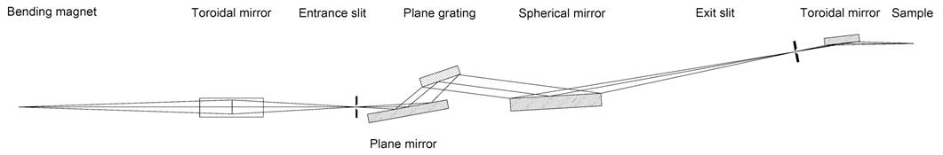
Figure 1.
Optical layout of
MSB, side view (not in scale).
End station
The key
component of the beamline is end station allowing not only experiments with
synchrotron light, but also in-situ sample treatment and its characterisation
by supplemental methods. In the experimental chamber it is possible to use Ar+
sputtering, LEED, HeI lamp for UPS, Mg+Al X-ray tube for XPS, various
evaporators and off-course sample heating and cooling during all experiments. High
pressure expositions and sample cleaning can be done in neighbouring
preparation chamber. Fast entry allows sample entering from ambient with
atmospheric pressure to the UHV chambers in 20 minutes.
Synchrotron
radiation photoemission spectroscopy
The main
experimental method used at MSB is photoemission spectroscopy. In contrast to
UPS, when excitation energy is 21.218 eV (HeI lamp) or XPS with excitation
energy 1253.6 eV (Mg K-α) and 1486.6 eV (Al K-α), the synchrotron radiation on MSB represents
a tuneable light source covering the whole gap between classical UPS and XPS. There
are more advantages – small and selectable energy bandwidth (10-500 meV) and focus
to the small spot on the sample (100 x 100 µm). The practical result is, that
synchrotron radiation in combination with SPECS Phoibos 150 electron energy
analyzer can distinguish not only between different elements, but also between
different sites of atoms by analyzing of chemical or surface core level shifts
only ~0.1 eV large. Tuning of excitation energy changes information depth (due
to variation of electron inelastic mean free path) as well as focusing on
specific element (due to photoionization cross section dependence). Near Edge
X-ray Absorption Fine Structure (NEXAFS) can be measured only with tuneable
photon source. Photon flux on the sample as a function of photon energy is
displayed on figure 2.

Figure 2. Photon flux as a function of photon
energy for resolving power E/dE = 2000.
Scientific
output
During its seven years history MSB produced nearly 50 scientific papers and other 10 are submitted or in press. As an example can be mentioned work about valence-charge fluctuations in the Pb/Si(111) system [3] or photoemission study of CO adsorption on ordered Pb/Ni (111) surface phases [4].
References
[1] http://www.elettra.trieste.it/accelerator/parameters.html
[2] R. Vašina, V. Kolařík, P. Doležel, M. Mynář, M. Vondráček, V. Cháb, J. Slezák, C. Comicioli and K.C. Prince, Nuclear Instruments and Methods in Physics Research A, 467–468 (2001) 561–564.
[3] V. Dudr, N. Tsud, S. Fabík, M. Vondráček, V. Matolín, V. Cháb and K.C. Prince, Physical Review
B, 70,
155334 (2004).
[4] V. Matolín, I. Matolínová, N. Tsud, S. Fabík, J. Libra, V. Dudr, V. Cháb
and K.C. Prince, Physical
Review B, 74,
075416 (2006).
Acknowledgements
Materials Science Beamline was supported by 3rd FP EU (CIPA-CT-0217), by Grant Agency of the Czech Republic (project GV202/98/K002) and by Ministry of Education of the Czech Republic (projects INGO LA 151 and LC06058).