Structure of GaAs whiskers grown on silicon nanowires
P. Klang1, A.M. Andrews1,2, H. Detz1, M.
Steinmaier2, A. Lugstein2, W. Schrenk1, G. Strasser3
1Center
for Micro- and Nanostructures, TU-Wien, Floragasse 7,
2Institute
for
klang@fke.tuwien.ac.at
The combination of silicon with III-V
semiconductors could offer the benefits of both material systems producing novel
structures for electronic and optoelectronic applications. We present the
hetero-epitaxial growth of single crystal GaAs whiskers on silicon nanowire
trunks forming structures with a 6-fold symmetry (see Fig. 1). The Si nanowires
on Si (111) substrates were prepared using a low pressure chemical vapor
deposition reactor and the vapor-liquid-solid growth mechanism. A 2 nm thick
layer of gold was sputtered on the surface as a catalyst for silicon nanowire
growth. We have grown GaAs nanowhiskers on these Si
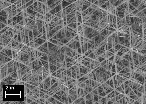
Figure 1. SEM picture of 6-fold GaAs whiskers on Si nanowire trunks visible after the deposition of 200 nm GaAs.
HRTEM brings us a direct view of the
crystal structure in the nanocrystals. The HRTEM cross-section of the Si
nanowires explains the 6-fold symmetry of the GaAs nanowhiskers observed by
SEM. The nanowhiskers grow perpendicular to the six side walls of the Si
nanowire trunks created by six
SEM technique provides us the information about the length and diameter of the nanowires. The length of our Si nanowires trunks are around 2 μm with a diameter determined by the Au catalyst, typically less than 100 nm. The length of the nanowhiskers grown on these nanowires depends mainly on the amount of deposited GaAs material and varies from several hundreds nm to several μm. It could be also shown that the GaAs nanowhiskers originate from any position along the Si nanowire trunks.
We used XRD to complement the TEM crystal structure analysis of our samples, with the advantage that it is non-destructive. We have measured reciprocal space maps with a wide ω/2Θ range (see Fig. 2) to find the powder diffraction peaks as well as the monocrystalline ones. The disadvantage of this method is the long measuring time required, but we obtain more information about the constituent materials. We compared different GaAs nanowhisker samples with the samples where only Si nanowires were grown to distinguish between the Si nanowire trunks and GaAs nanowhiskers. We identified monocrystalline Si, polycrystalline wurtzite GaAs, due to the distributed orientation of the single crystal nanowhiskers with respect to each other, Au and also the AuGa alloy.
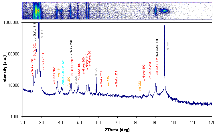
Figure 2. X-ray RSM and projection to 2Θ/ω axis measured on sample with 200 nm equivalent layer thickness of GaAs grown on silicon nanowires.
We confirmed the wurtzite structure of the GaAs whiskers grown on Si nanowires by the XRD technique and additionally showed the presence of the AuGa alloy, a possible catalyst for the nanowhisker growth. The characterization of the sample structure and growth mechanism of GaAs nanowhiskers on Si nanowire trunks moves us closer to novel Si:III-V hetero-epiataxial devices.
References
1. A.
Lugstein, A.M. Andrews, M. Steinmair, Y. Hyun, E. Bertagnolli, M. Weil, P.
Ponratz, M. Schramböck, T. Roch, G. Strasser, Nanotechnology, 18,
(2007), 355306