Growth of nanocrystalline magnetron
sputtered TiO2 thin films studied by X-ray scattering
R. Ku×el1, L. Nichtovß1,
Z. Matņj, D. He°man2, J. Musil2
1Faculty
of Mathematics and Physics, Charles University in Prague, Czech Republic;
2Faculty of Applied Sciences, University of West Bohemia in Pilsen, Czech Republic
Titanium dioxide films
are widely used because of their excellent properties as chemical stability,
mechanical hardness and optical transmittance with high refractive index. The photocatalytic activity of TiO2
can result in the decomposition of organic compounds on the TiO2
surface or the reduction of the contact angle between water and the TiO2
surface under ultraviolet irradiation. The films can be prepared by several
techniques but the magnetron deposition is favourable from the point of view of
mechanical durability required for practical applications. Depending on the
deposition conditions, the films can be prepared as amorphous or
nanocrystalline.
In the present work, a
complex XRD study was performed on the films sputtered by dual magnetron on the
glass and single-crystal silicon substrates. A set of nanocrystalline films
with different thickness in the interval of 0.1 mm to 2 mm was investigated after the deposition. The
measurement was performed onĀ Philips
X'Pert MRD in parallel beam setup, 2q scans with very low angles of incidence with
collimators and Goebel mirror in the primary beam. X-ray reflectivity curves
were measured too.Ā The curves dropped
rapidly for all the samples except the thinnest one (0.1 mm). In addition, contact angles of water drops on
the film surface were measured after different periods of films irradiation by
UV light.
The films deposited on
glass subrate shown similar behaviour to the ones on Si substrate in many cases
but there are also significant differences. The films on silicon show usually
more pronounced texture. The most important differences were found in the phase
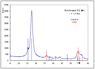
composition for the thinnest samples, though. The thinnest film (0.1 mm) on glass substrate was amorphous while for the
same film on silicon clear broad peaks of rutile were detected. Similarly, for
the film with the thickness of 0.2 mm (Fig. 1a) for which small rutile peaks can also
be seen on glass substrate. For none of these thin films any significant
decrease of the drop contact angle after UV irradiation was found even though
there are visible differences in their surface roughness. The angles remained
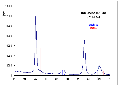
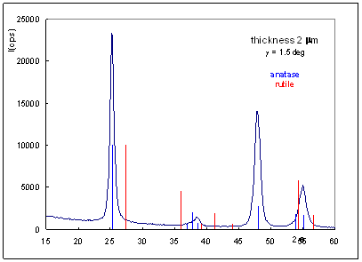
on high values (65 - 75░). For the films thicker than 0.5 mm, anatase is clearly dominating phase (Fig. 1b,
1c) and for the 2 mm thick
film only pure anatase was detected.
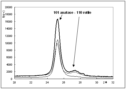
A set of measurements
with different angles of incidence 0.5 ¢ 5░ and consequently also different
penetration depths (the penetration depth for the smallest angle of incidence
is below 200 nm) clearly show that rutile grows on the interface with both Si
and glass substrates in all cases but its growth is supressed for thicker films
by anatase which is mainly on the top (Fig. 1d). Since for all the thicker
films the angles of water drops were drastically reduced after UV irradiation
(5 hrs irradiation, down to 10 ¢ 20░), it seems that only anatase is favourable
in this case for hydrophilicity and by contrast rutile makes films hydrophobic.
Differences between both substrates were also found. The films on silicon have
better hydrophilicity than corresponding films on glass. From the structural
point of view, the former have slightly better crystallinity and more
pronounced texture.
Because of very broad
peaks, the detailed measurement of residual stresses could be performed on the
Eulerian cradle by the sin²ψ method only for two different peaks of
anatase phase (101, 200). The dependences were strongly curved but with the
absence of splitting for negative and positive inclination angle which could
indicate triple-axis stresses. The curvature can be ascribed to the texture. The
pltos are also very different for both peaks. For the peaks 101 and 200 the
pole figures have also been measured and shown the presence of (100) texture.
The texture was not completely fiber and for samples on Si it was significantly
inclined with respect to the surface (Fig. 2). The asymmetry of the texture can
be well understood, if we take into account that the deposition was made by
dual magnetron.
This work is supported by the Grant Agency of the
Czech Republic, no. 106/06/0327.
|
|
|
|
a) |
b) |
|
|
|
|
c) |
d) |
|
Fig.
1. Diffraction
patterns of TiO2 films with different thickness ¢ a) 0.1 mm, b) 0.5 mm, c) 2 mm. The patterns were obtained in parallel beam optics and 2q scan and fixed angle of incidence ¢ 1.5º. In Fig. 1d) ¢ patterns
from the sample with the thickness 0.9 mm, obtained at different angles
of incidence ¢ lower thick line - 0.5º, middle thin line - 1.0º,
upper thick line - 1.5º. Thick bars indicate theoretical peak positions
for anatase, thin bars correspond to the peaks of rutile. |
|
|
|
|
|
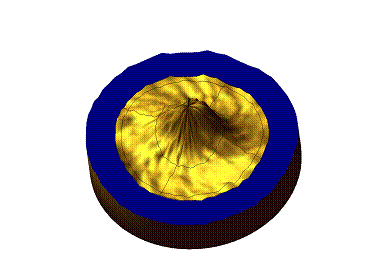
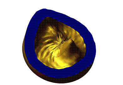
Fig.
2. Pole figure
200 for the sample 2 mm thick. The asymmetry of the
texture can be seen in 2.5D plot (left) as well as the inclination of the
texture on Si substrate. |
|