Spatial μm-resolved structure characterization of semiconductor wafers and lateral overgrowth structures by synchrotron radiation rocking curve imaging
P. Mikulík1, D. Lübbert2,3, L. Helfen2, P. Pernot2, S. Keller4, T. Baumbach2
1Institute of Condensed Matter Physics, Masaryk University, Brno, Czech Republic
2ANKA / Institute for Synchrotron Radiation, Forschungszentrum Karlsruhe, Germany
3Humboldt-Universität, Berlin, Germany
4University of California at Santa Barbara, CA, USA
mikulik@physics.muni.cz
We present recent advances on local lattice and structure quality control of semiconductor wafers and overgrown structures with spatial resolution down to one micrometer over an extended sample area. We employ synchrotron radiation diffraction rocking curve imaging (RCI) technique, which combines digital X-ray topography and conventional Bragg-diffraction rocking curve recording. Application of this method has been pushed from qualitative wafer structure characterization towards quantitative mapping of local crystalline misorientations and dislocation density and towards one-micrometer spatial resolution to study crystalline morphology of overgrown patterned structures [1,2,3].
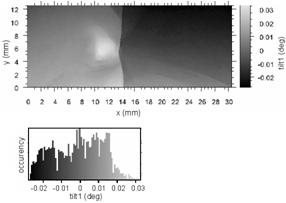
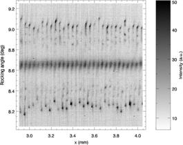
Growth of compound materials in ingots, like SiC, GaAs, GaN, InP, leads to inherited imperfections. Regions of specific misoriented macrodefects and dislocation regions in ingots can be qualitatively mapped by RCI [1], see figure 1. Epitaxial lateral overgrowth (ELO) is an innovative crystal growth technique expected to achieve a better crystal quality. The overgrown layer shows significantly lower density of threading dislocations than in the wetting layer. With micrometer-resolved 2D detector, the RCI allows to monitor the lattice quality and lattice tilts in individual periods of the structure [2], see figure 2. Significant information can be obtained from individual sample areas as small as 2 micrometers in all three spatial dimensions, and to check the findings of double-crystal diffraction rocking curve measurements.
|
|
|
|
Figure 1. A lattice tilt component distribution in a specific area on a GaAs wafer [3]. |
Figure 2. Angular separation of the GaN ELO column vs. wings (centre vs. top and bottom spots) [3]. |
References
[1] P. Mikulík, D. Lübbert, D. Korytár, P. Pernot, and T. Baumbach, J. Phys. D: Appl. Phys., 36, (2003), A74.
[2] D. Lübbert, T. Baumbach, P. Mikulík, P. Pernot, L. Helfen, R. Köhler, T.M. Katona, S. Keller, S.P. DenBaars, J. Phys. D: Appl. Phys., 38, (2005), A50.
[3] P. Mikulík, D. Lübbert, P. Pernot, L. Helfen, T. Baumbach, Appl. Surf. Sci., (2006), in print.