X-ray diffraction from polycrystalline multilayers with flat interfaces in grazing-incidence geometry
P. F. Fewster, N. L. Andrew
PANalytical Research Centre, Sussex Innovation Centre, Falmer, Brighton, UK
V. Holý
Department of Physics of Electronic Structures, Charles University, Prague, Czech Republic
K. Barmak
Department of Materials Science and Engineering, Carnegie Mellon University, Pittsburgh, U.S.A.
J. Krčmář
Institute of Condensed Matter Physics, Masaryk University, Brno, Czech Republic
I. INTRODUCTION
X-ray powder difractometry is a standard method for obtaining the size of crystallites in industrial materials. However in general the method is suited to obtaining the size normal to the surface using the focusing Bragg-Brentano geometry. To estimate the general shape of crystallites in bulk samples, several reflections are required, however this method is less suited to thin films that in general exhibit significant texture. Hence these methods are essentially bulk methods, i.e. they assume a random distribution of orientations and become difficult in the analysis of thin films when the crystallite size in the plane of the interface cannot be determined. Access to scattering planes normal to the interface is possible at grazing angles of incidence. This in-plane scattering geometry relies on the refractive index of X-rays being less than unity, such that there is a critical angle for total external refection. Thus the X-rays can enter through the sample surface, scatter from planes normal to the surface plane and then scatter out through the same surface. By varying the angle of incidence the penetration depth is varied. This has been used extensively in the study of mono-crystalline semiconductor wafer samples and can also be shown to work for very thin (30nm) polycrystalline layers. Although some average crystallite size is determined, knowledge of the variation as a function of depth in thin films can be very valuable.
This paper describes a new method to measure
the crystallite size and its distribution as a function of depth in multi-layer
thin films. The principle relies on the idea that when X-rays are scattered at
an interface the incident and scattered waves create a standing wave whose
periodicity can be varied and thereby enhance the scattering at certain
depths.
II. THEORETICAL DESCRIPTION
In the in-plane grazing-incidence geometry, both the angle of incidence αi of the incident radiation, and the angle of exit αf of the scattered beams are comparable with the critical angle αc of total external reflection of x-rays (Fig. 1). Thus, the interaction of x-rays with matter is rather strong and it cannot be described by a simple kinematical approximation. On the other hand, the polycrystalline grains can be assumed much smaller than the extinction length τ of x-rays in the material, so that the individual grains scatter kinematically.
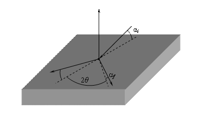
Fig. 1: Grazing incidence diffraction, the crystallographic plane is perpendicular to crystal surface.
We describe the scattering process using the
distorted-wave Born approximation (DWBA) [1], in which the total scattering
potential ![]() occurring in the wave equation:
occurring in the wave equation:
![]() (1)
(1)
is divided in two terms ![]() The first term
describes the undisturbed system, the latter is the disturbance. Within the
DWBA, the undisturbed wave equation with
The first term
describes the undisturbed system, the latter is the disturbance. Within the
DWBA, the undisturbed wave equation with ![]() is solved exactly,
while the scattering from
is solved exactly,
while the scattering from ![]() is assumed kinematical.
is assumed kinematical.
In simple model with flat interfaces ![]() corresponds to an amorphous multi-layer and we
assume that the primary x-ray beam Ei is scattered by
corresponds to an amorphous multi-layer and we
assume that the primary x-ray beam Ei is scattered by ![]() which generates a
standing wave-filed
which generates a
standing wave-filed ![]() in the
multi-layer; this wave-field is diffracted in the polycrystalline grains due to
in the
multi-layer; this wave-field is diffracted in the polycrystalline grains due to
![]() . The diffracted wave-field,
. The diffracted wave-field, ![]() is scattered again
by
is scattered again
by ![]() and finally, the
measured wave-field Ef results. In this choice, we completely
neglect the scattering from interface roughness.
and finally, the
measured wave-field Ef results. In this choice, we completely
neglect the scattering from interface roughness.
We assume a sample consisting in N
layers. The wave-field ![]() in layer j is generated by the incident
wave Ei consists of transmitted and reflected components and
their amplitudes can be calculated using the well-known matrix formalism [2].
The second, independent solution
in layer j is generated by the incident
wave Ei consists of transmitted and reflected components and
their amplitudes can be calculated using the well-known matrix formalism [2].
The second, independent solution ![]() of Eq. (1) (where
of Eq. (1) (where![]() ) is chosen so that its vacuum incident wave equals the
actual scattered wave Ef and this solution is time inverted.
) is chosen so that its vacuum incident wave equals the
actual scattered wave Ef and this solution is time inverted.
The diffuse part of differential cross-section of the diffraction from polycrystalline grains is [1]:
![]() , (2)
, (2)
where ![]() denotes the
averaging over a statistical ensemble of random positions Rjn (position vector of grain n in layer j), of the grains,
random directions of hjn
(reciprocal lattice vector of grain), and over random grain sizes. The
matrix elements υB
is:
denotes the
averaging over a statistical ensemble of random positions Rjn (position vector of grain n in layer j), of the grains,
random directions of hjn
(reciprocal lattice vector of grain), and over random grain sizes. The
matrix elements υB
is:
![]() , (3)
, (3)
and disturbance ![]() comprises the
crystal structure of individual polycrystalline grains
comprises the
crystal structure of individual polycrystalline grains
III. NUMERICAL EXAMPLES
In the simulations, we have assumed the multi-layer consists of 14 periods, each contains a 4 nm thick Nb layer and a 11 nm thick Al layer. We also assume that the polycrystalline grains are spherical, each grain has the same radius R, grain positions are completely uncorrelated, all grain orientations have the same probability (no texture).
Figure 2 shows an intensity map calculated in
the coordinates (2θ; αi), assuming αf
= 0,5° where 2θ is the in-plane scattering
angle. In this map, a part of the Debye ring of Nb110 and Al220 is depicted.
The width of the ring in the 2θ direction is inversely
proportional to the grain radius R. Along the Debye ring, the intensity
modulation follows the dependence of the intensity of the wave-field ![]() on αi; the period of the
modulation is inversely proportional to the multi-layer period. The rings Nb110
and Al220 have different structures; these differences are caused by different
intensities of the standing wave in Nb and Al layers. Below αc,
the penetration depth of the incoming beam is very small and no diffraction
from the grains takes place.
on αi; the period of the
modulation is inversely proportional to the multi-layer period. The rings Nb110
and Al220 have different structures; these differences are caused by different
intensities of the standing wave in Nb and Al layers. Below αc,
the penetration depth of the incoming beam is very small and no diffraction
from the grains takes place.
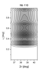
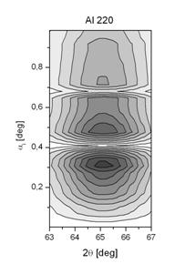
Fig. 2: Calculated intensity for Nb110 and Al220, mean grain size R = 2 nm, αf = 0,5°.
Figure 3 shows the intensity scans for 2θ = const. calculated for Nb110 and Al220 diffraction and reflection on assuming multi-layer:
Fig.3: The intensity scans for 2θ = const. for Nb110 and Al220 and reflection on multi-layer, mean grain size R = 2 nm, αf = 0,5°.
IV. DISCUSSION
Model with flat interfaces (and expectations in paragraph III.) is too simplified to describe real experimental data. The most important point of the further work is description of the scattering process from interfaces roughness. The next problems are the texture, influence of the random size of the grains, etc.
Reference:
[1] S.K. Sinha, E.B. Sirota, S. Garoff, and H.B. Stanley, Phys. Rev. B 38, 2297 (1988).
[2] V. Holý, U. Pietsch, and T. Baumbach, High Resolution X-Ray Scattering from Thin Films and Multilayers, (Springer, Berlin 1999).