Advanced X-ray
Diffraction Imaging Techniques
for Semiconductor
Wafer Characterisation
P. Mikulík1,
T. Baumbach1, D. Korytár1, P. Pernot1, 2, D.
Lübbert1, 2, L. Helfen1, 2,
Ch. Landesberger3
1Fraunhofer-Institut
für Zerstörungsfreie Prüfverfahren,EADQ, Dresden, Germany
2European
Synchrotron Radiation Facility, Grenoble, France
3Fraunhofer-Institut für Zuverlässigkeit und Mikrosystemtechnik, Munich,
Germany
Wafer quality inspection and defect analysis are
crucial for improvements of the wafer fabrication technology as well as the
correlation of device properties with the processes of wafer treating. This
work demonstrates trends of high-resolution X-ray diffraction imaging
techniques with synchrotron radiation sources and the capability of detailed quality
inspection of wafers concerning their structural perfection. We apply these methods to visualise and to characterise the
defects and deformations induced by growing, cutting, grinding, etching and
gluing in the production of semiconductor wafers (in particular Si and GaAs
wafers) and in ultra-thin silicon wafers. We present synchrotron topography and
synchrotron area diffractometry methods to analyse qualitatively and
quantitatively: dislocations and lineages, micro-defects and micro-cracks,
wafer tilts and warpages, tensor of local lattice rotations.
1. Defects and
deformations induced by grinding and gluing of ultra-thin silicon wafers.
Thin semiconductors are used for power devices, chip
card application and high frequency integrated circuits (ICs) and
opto-electrical components. Current trends in thin chip technology are
targeting extremely low packaging heights and thin and flexible ICs for smart
labels and highly integrated chip systems for multifunctional devices. Until
today the chip thickness of the ICs is limited to the range of 100 to
200 µm. Completely new applications appear when wafer thinning, dicing and
die mounting technology is extended to ultra thin chips with a remaining
thickness of 10–30 µm [1]. In this range silicon substrates become
mechanical flexible and new products like laminate mounted "Smart
Labels" become reality, see figure 1.
Wafer thinning approaches rely on a coarse grinding
process to remove of the wafer about 300 µm silicon bulk. Further
micro-thinning (grinding, spin and plasma etching) removes the additional
material and eliminates the stress resulting from micro-defects. Damaged
subsurface zones extending 5–15 µm into the substrate have to be removed
by chemical etching. Finally, the chemical-mechanical polishing step reduces
the roughness and cleans the surface.
Synchrotron X-ray diffraction imaging techniques prove
their value for research and industry in characterisation of grown-in and
process-induced defects as well as stresses. Here we study the surface and volume
damage introduced by the grinding and the damage removal by subsequent surface
treatment mentioned above, as well as the detection of lattice distortion
fields generated by the gluing of the ultra-thin wafer on a target wafer. The
main results have been obtained by:
a)
X-ray
monochromatic section topography in Bragg case with a high sensitivity
specially to (sub-micrometer) defects using the visibility of Pendellösung
fringes,
b)
high resolution
monochromatic double crystal topography with a high sensitivity in particular
to strain and to diffuse scattering at the tails of rocking curves,
c)
the quantitative
imaging of lattice deformations and macroscopic defects by micrometer resolved
tilt maps.
The main results concerning the grinding damage
and its removal by spin etching are:
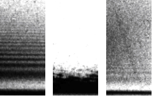
1. Etching-off or polishing-off (CMP) only
5 µm
thick surface layer after grinding is sufficient to remove the surface damage
significantly so that the Pendellösung fringes are restored to a high degree.
However, full restoration of the visibility of fringes was not observed even
after etching and polishing removal of 50 µm, see figure 2.
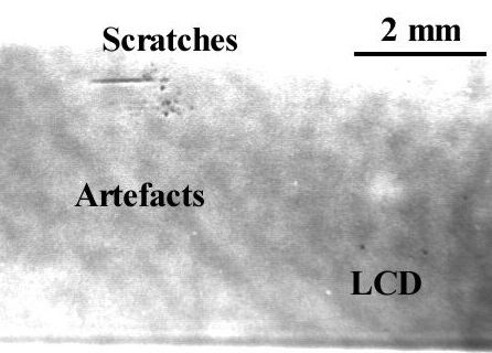
2. Low density (<1000 cm-2)
of larger (<20–80 µm)
low contrast defects (LCD) remain also after etching-off 20 µm of surface layer, see figure 3.
The qualitatively and
quantitatively imaging of lattice tilt induced by the glue attaching the
thin wafer to the carrier wafer has been performed by white beam section
topography and lattice tilt mapping by the area diffractometry method discussed
in more details in the following section.
2. µm-resolved
determination of the three-dimensional lattice misorientation for the semiconductor
wafers inspection by synchrotron radiation area diffractometry.
Wafer fabrication technology of compound materials
such as GaAs, InP, SiC, CdZnTe requires up-to-date structure characterisation
methods and defect analysis methods in order to achieve high quality wafers for
micro-electronic applications. GaAs, for example grown by LEC method, can form
columnar structures with highly perfect crystalline structure inside the
crystallites. This can be observed optically on etched wafers as a presence of
lineages, dislocations, and other defects on the boundaries. Furthermore, a
growth inhomogeneity can lead to nucleation of specific misoriented
crystallite-like defects with lattice planes tilted with respect to the main
substrate lattice which cause problems during subsequent epitaxy steps.
In an earlier work [2] we developed a method of
µm-resolved synchrotron X-ray area diffractometry as a tool for wafer quality
characterisation by combining digital topography and conventional wafer
Bragg-diffraction rocking curves. Recently we have extended this method to
reveal the complete three-dimensional tensor of local lattice misorientation in
wafers, including so-called macrodefects of large rotation angles with respect
to the undisturbed region [3].
Acknowledgements
P.M. and D.K. acknowledge support by the Marie Curie
Fellowship of the European Community, program "Human Potential"
(contract nb. MCFI-2000-00671) and
"Growth" (G5TR-CT2000-00046), respectively.
References
[1] C. Landesberger, G. Klink,
G. Schwinn, R. Aschenbrenner, Advanced Packaging Materials,
Processes, Properties and Interfaces, Proceedings of IEEE 01TH8562, ISBN
0-930815-64-5, pp. 92–97.
[2] D. Lübbert, T. Baumbach,
J. Härtwig, E. Boller, E. Pernot, Nucl. Inst. Meth. Phys. Res. B 160 (2000) 521.
[3] P. Mikulík, T. Baumbach, D. Korytár, D. Lübbert,
P. Pernot, submitted.
=============== FIGURES
==================
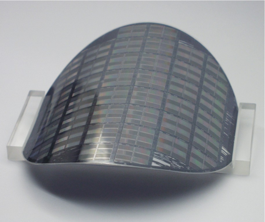
Figure 1.
Include graphics: mikulik_figure1.jpg
Caption: Ultra-thin silicon wafers become mechanical
flexible.
Figure 2.
Include graphics: mikulik_figure2.png
Caption: Sub-surface damage characterisation by
Pendellösung
fringes: reference Si wafer (left), ground wafer (middle), ground and 46 mm etched wafer
(right).
Figure 3.
Include graphics: mikulik_figure3.jpg
Caption: Monochromatic projection topography of a
80 mm thick Si wafer (grounded and etched).
Figure 4.
Include graphics: mikulik_figure4.png
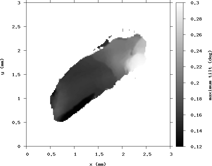
Caption: Distribution of maximum of the lateral
lattice misorientation value along a defective area in a GaAs wafer.
FIGURE PREVIEW:
1.  2.
2.  3.
3.  4.
4.