Hexaferrite thin films grown by chemical solution deposition on differently oriented sapphire substrates
Radomír Kužel1, Lukáš Horák1, Milan Dopita1, Darina Smržová2, Josef Buršík2
1Charles University, Faculty of Mathematics and Physics, Prague, Czech Republic
2Institute of Inorganic Chemistry of the Czech Academy of Sciences, v.v.i., 250 68 Husinec-Řež 1001, Czech Republic
lukas.horak@matfyz.cuni.cz
Strongly oriented ferrite films were deposited on several substrates by chemical solution deposition, and different substrate/seeding layer/ferrite layer architectures were designed [e.g.1, 2]. In previous experiments, the hexaferrite films were deposited on STO (SrTiO3) substrates with orientations (111), (110), (100), and ceramics. In all cases, (00l) textures of Y-phases of different degrees were observed, but only for the (111) substrate strong in-plane texture was found. For other used substrates, usually some intermediate seeding layer was necessary to obtain good orientation of Y-films. The most successful were LaAlO3 and MgO substrates.
In this work [3], highly oriented M-phase
films with different orientations were grown on Al2O3 (![]() - a-cut, (0001)
– c-cut, (
- a-cut, (0001)
– c-cut, (![]() - m-cut and (
- m-cut and (![]() - r-cut single crystal
substrates. A procedure involving thin and the difference in lattice parameters
between the seed and bulk layers. SrFe6Ga6O12
seed layers was adopted to modify the lattice mismatched interface between film
and substrate and allow the growth of oriented films. Usual thickness of the
seeding layer was about 100 nm obtained after several deposition cycles.
M-phase, SrFe12O19, film samples with 1600 nm thickness
were used for different analyses. The deposition of the bulk M layer always reduces
the in-plane orientation (while maintaining the epitaxial relationship) of the
originally well-oriented M seed layer. The deposition of the bulk layer M
usually results in a broadening of the j and w scan peaks by
about a factor of two in most cases. The increase in FWHM value for the w scan observed
in the case of the M-bulk layer suggests a slight increase in misorientation of
the layer and deterioration of the OP orientation of the M phase due to the
increasing total layer thickness the difference in lattice parameters between
the seed and bulk layers
- r-cut single crystal
substrates. A procedure involving thin and the difference in lattice parameters
between the seed and bulk layers. SrFe6Ga6O12
seed layers was adopted to modify the lattice mismatched interface between film
and substrate and allow the growth of oriented films. Usual thickness of the
seeding layer was about 100 nm obtained after several deposition cycles.
M-phase, SrFe12O19, film samples with 1600 nm thickness
were used for different analyses. The deposition of the bulk M layer always reduces
the in-plane orientation (while maintaining the epitaxial relationship) of the
originally well-oriented M seed layer. The deposition of the bulk layer M
usually results in a broadening of the j and w scan peaks by
about a factor of two in most cases. The increase in FWHM value for the w scan observed
in the case of the M-bulk layer suggests a slight increase in misorientation of
the layer and deterioration of the OP orientation of the M phase due to the
increasing total layer thickness the difference in lattice parameters between
the seed and bulk layers
The pseudo-epitaxial growth and orientation relation were verified by X-ray diffraction texture analysis and reciprocal space mapping. j and w scans as well as selected pole figures were measured in low-resolution parallel beam setup with polycapillary in primary beam and parallel plate collimator (Panalytical MRD), monochromator and point detector in the secondary beam. Significant out-of-plane textures of (h00), (00l), and (hh0) were found on the a-, c- and m-cuts of substrates, respectively. The FWHM of w-scans were 0.8-1.2°. Similarly, significant in-plane orientations were found for the a- and m-cuts of the substrates, respectively while for the c-cut they were less good indicating a quite large fraction of unoriented crystallites. The surface morphology at room temperature using AFM in tapping mode. Except for the c-cut substrates, the surface structure is formed by parallel aligned grains with high aspect ratio and the shortest dimension along c-crystallographic axis. The FWHM of the w-scans depends strongly on j angle being the highest along this smallest crystallite dimension which could be caused by the size effect. However, to decide this, the Williamson-Hall plots for w-scans were measured for more diffraction orders. They were also constructed in classical form, i.e. for the profiles measured along the diffraction vector (q-2q). These measurements were performed in higher-resolution setup with hybride Ka1 monochromator in the primary beam and Pixcel 3D detector in the secondary beam.
For w-scans, it is clear, that crystallite misorientations (slope) is still the dominating effect for broadening and it is more significant in the direction perpendicular to crystallite rod, i.e. along [0001]. The intercepts would give crystallite size of 30 to 50 nm for m- and c-cut of subtrates, respectively (Figure 1). This corresponds quite well to AFM pictures. Classical WH plots along the diffraction vector gives small microstrains of about 0.06 to 0.1 % and crystallite size above 100 nm.
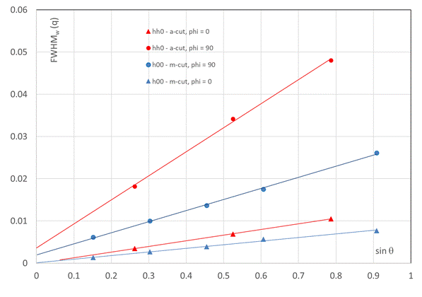
Figure 1. Williamson-Hall plot of the width of w-scans of hh0 and h00 diffractions for m-cut and a-cut substrates, respectively and for two orientations of the film, along (j = 0°) and perpendicular (j = 90°) to crystallite rods.
For M layers on r-cuts of substrates, the orientation is more complex and in original measurements no intensity in symmetrical scans could be observed. However, pole figure 114 showed that actually there is an inclined texture with inclination 3-5 ° depending on the film (Figure 2) and the case was studied in detail [4].
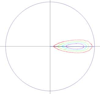
Figure 2. Pole figure 114 of the M-film on r-cut substrate. The circle corresponds to the angle c of 10°.
A comparison of texture analysis results obtained on sapphire substrates of different cuts shows that the mutual orientations of the crystal structure of the M film and the sapphire substrates in epitaxial structures are always the same (except for a small angle deviation for an r-cut). As a result, there is a high probability that thin films of the M hexaferrite film with an easy axis of magnetization at any angle with respect to the substrate can be attained by making an appropriate choice of the orientation of the Al2O3 substrate.
[1] KW. Shin, M. Soroka, A. Shahee, KH Kim, J Buršík, R. Kužel, M. Vronka, MH Aguirre: Advanced Electronic Materials. v. 8 (2022). 2101294.
[2] M. Soroka, J. Buršík, R. Kužel, L. Horák, J. Prokleška, M. Vronka & V. Laguta. J. Eur. Ceram. Soc. (2023). 43, 6916-6924.
[3] D. Smržová, J. Buršík, L. Horák, R. Kužel, V. Laguta, J. Vít, & O. Laguta. J. Eur. Ceram. Soc., submitted for publication.
[4] L Horák, R. Kužel, M. Dopita, J. Buršík, Materials Structure, vol 32 (2026), this issue
The authors appreciate the support by the grant of the Czech Grant Agency, no. 24-12710S.