Substrate-Controlled Crystallization and Crystal Orientation of HMTP Organic Semiconductor Thin Films on Graphene/SiC
Devanshu Varshney,1 Pavel Procházka,2 Veronika Stará,2 Mykhailo Shestopalov,3 Jan Kunc3, Jan Čechal2,4 , Jiří Novák1
1Department of Condensed Matter Physics, Faculty of Science, Masaryk University, Kotlářská 2, 61137 Brno, Czech Republic
2CEITEC - Central European Institute of Technology, Brno University of Technology, Purkyňova 123, 612 00 Brno, Czech Republic.
3Charles University, Faculty of Mathematics and Physics, Institute of Physics, Ke Karlovu 5, 121 16, Prague 2, Czech Republic
4Institute of Physical Engineering, Brno University of Technology, Technická 2896/2, 616 69 Brno, Czech Republic.
We investigate thin films of the π-conjugated electron-donor organic semiconductor molecule 2,3,6,7,10,11-hexamethoxytriphenylene (HMTP) on two structurally similar surfaces: single-layer graphene (SLG) on SiC(0001) and the buffer layer on SiC(0001) [1]. Epitaxial graphene on SiC consists of an sp²-hybridized single-layer graphene above a carbon buffer layer. Although the buffer layer retains a graphene-like lattice, it is partially sp³-bonded to the underlying Si atoms of the SiC substrate, creating a locally inhomogeneous surface at the nanoscale [2]. In this talk, I will show how these two structurally similar surfaces control both the crystallization and the crystal orientation of HMTP organic semiconductor thin films from the earliest stages of growth.
We combine low-energy electron microscopy
and diffraction (LEEM/LEED), which probe the initial growth, with a set of
X-ray diffraction techniques — pole figure measurements, azimuthal scans,
symmetric ω/2θ scans, and rocking curve measurements — to
characterize the crystallographic texture and crystal quality of films up to
approximately 30 nm thickness on both surfaces. On SLG, pole figures measured
for HMTP {![]() reflections
reveal two sets of six sharp diffraction spots, confirming highly ordered
epitaxial growth with two mirror domains rotated by ±19.1° relative to the
graphene lattice (fig.1(a)). Azimuthal scans show narrow peaks with a full
width at half maximum of 0.5°, close to the instrumental resolution,
demonstrating exceptional in-plane orientational order. Symmetric scans further
reveal that the HMTP {
reflections
reveal two sets of six sharp diffraction spots, confirming highly ordered
epitaxial growth with two mirror domains rotated by ±19.1° relative to the
graphene lattice (fig.1(a)). Azimuthal scans show narrow peaks with a full
width at half maximum of 0.5°, close to the instrumental resolution,
demonstrating exceptional in-plane orientational order. Symmetric scans further
reveal that the HMTP {![]() lattice planes
are parallel to the sample surface, while the presence of Laue oscillations
confirms uniform film thickness and high crystalline coherence.
lattice planes
are parallel to the sample surface, while the presence of Laue oscillations
confirms uniform film thickness and high crystalline coherence.
In contrast, HMTP films grown on the buffer
layer exhibit a ring-shaped band of enhanced intensity with slight azimuthal
modulation in the pole figure measured for the HMTP {![]() reflections
(fig.1(b)). The corresponding azimuthal scans show maxima that are
approximately 20 times weaker and significantly broader than those observed on
SLG, accompanied by a higher continuous intensity profile between the maxima.
This indicates a large fraction of randomly oriented crystalline domains.
During the initial growth stages, HMTP grows amorphously; however, with
increasing film thickness, it evolves into a polycrystalline film with only
weak orientational order with respect to the substrate. Furthermore, symmetric
scans show that the HMTP {
reflections
(fig.1(b)). The corresponding azimuthal scans show maxima that are
approximately 20 times weaker and significantly broader than those observed on
SLG, accompanied by a higher continuous intensity profile between the maxima.
This indicates a large fraction of randomly oriented crystalline domains.
During the initial growth stages, HMTP grows amorphously; however, with
increasing film thickness, it evolves into a polycrystalline film with only
weak orientational order with respect to the substrate. Furthermore, symmetric
scans show that the HMTP {![]() lattice planes
are parallel to the sample surface, as observed for HMTP on SLG. However, the
absence of Laue oscillations and the lower peak intensity signify reduced
crystalline quality.
lattice planes
are parallel to the sample surface, as observed for HMTP on SLG. However, the
absence of Laue oscillations and the lower peak intensity signify reduced
crystalline quality.
Finally, we decouple the buffer layer via hydrogen intercalation, which breaks the Si–C bonds and converts the buffer layer into quasi-freestanding graphene [3]. Subsequent growth of HMTP on this surface leads to epitaxial films, demonstrating that the unevenly distributed covalent Si–C bonding between the buffer layer and the SiC substrate is the decisive factor limiting organic semiconductor thin-film crystallinity on graphene/SiC.
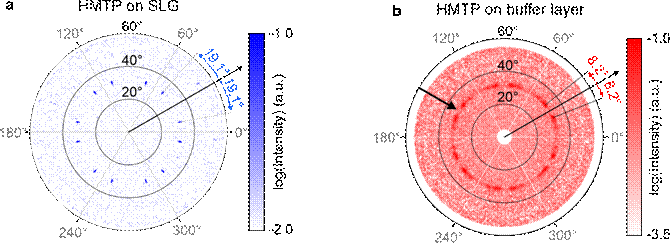
Figure 1: XRD pole
figures of the HMTP { reflections
measured for the fims grown on SLG (a) and on the buffer layer (b). The sharp
diffraction spots in (a) and the ring-shaped band of enhanced intensity in (b),
indicated by the arrow, are both located at a polar angle of 31.7° with respect
to the HMTP [0001] direction.
reflections
measured for the fims grown on SLG (a) and on the buffer layer (b). The sharp
diffraction spots in (a) and the ring-shaped band of enhanced intensity in (b),
indicated by the arrow, are both located at a polar angle of 31.7° with respect
to the HMTP [0001] direction.
[1] Varshney, D.; Procházka, P.; Stará, V.; et al. Interfacial Coupling Controls Molecular Epitaxy of HMTP on Graphene/SiC. ACS Applied Materials & Interfaces 2026.[Unknown A1]
[2] Backes, C.; Abdelkader, A. M.; Alonso, C.; et al. Production and Processing of Graphene and Related Materials. 2D Mater. 2020, 7, 022001.
[3] Kunc, J.; Rejhon, M.; Hlídek, P.; et al. Hydrogen Intercalation of Epitaxial Graphene and Buffer Layer Probed by Mid-Infrared Absorption and Raman Spectroscopy. AIP Adv. 2018, 8, 045015.