X-ray diffraction from epitaxial thin films : an analytical expression of the line profiles accounting for microstructure
A. Boulle, R. Guinebretière, A. Dauger
Science des Procédés Céramiques et de Traitements de Surface – CNRS UMR 6638
ENSCI, 47 à 73 avenue Albert Thomas 87065 Limoges Cedex
The effect of finite crystal size on the X-ray diffraction line profiles is known since the experiment of Friedrich, Knipping and Laue [1] who first derived the formula known as the Laue function : sin²(Qt/2)/sin²(Qd/2), where Q, t and d are the length of the scattering vector, the crystal thickness and the interplanar spacing in the direction of the scattering vector. Since that time a large amount of work has been devoted to the extraction of information concerning ‘size’ and ‘strain’ from the XRD line profiles [2,3], with particular emphasis being laid on polycrystalline materials. In such systems the kinematical theory of diffraction was shown to apply very well. Concerning epitaxial thin films, the high crystalline quality layers that are achievable using molecular beam epitaxy or chemical vapor deposition strongly promoted the use of the more rigorous dynamical theory of diffraction [4]. Up to recently these studies mainly focused on semiconductor materials.
In the recent years much attention has been paid on oxide epitaxial thin films, but real structure effects (e.g. random lattice spacing fluctuations, thickness fluctuations, roughness…) remain difficult to incorporate into the dynamical scattering theory. Moreover, the relative imperfection of oxide thin films (as compared to semiconductors) enables to use the kinematical theory. However, the presence of defects strongly alters the shape of the intensity distribution predicted by Laue. Several authors modified this expression in order to account for the effect of one of the above-mentioned defect [5,6], but up to now the combined effects of different defects are in general handled using a numerical integration of the expression of the intensity distribution.
In this communication we derive an analytical interference function able to describe the XRD line profiles of an epitaxial thin film with a microstructure made of different type of defects: film thickness fluctuation, roughness, cumulative and non-cumulative random lattice spacing fluctuations. The derivation is carried-out within the framework of the kinematical scattering theory. For brevity, in this abstract we focus on the coherently scattered intensity, I = <E><E*>. The effect of diffuse scattering will be discussed at the conference. The scattered amplitude distribution, <E>, of a thin film with a rough interface and a fluctuating thickness can be written [7]:
![]()
qz is the z-component of the reduced
scattering vector q = Q – h, h being the reciprocal
lattice vector of the reflection (the z axis is chosen parallel to the outwards
film surface normal). t, zI W and Fh are the film thickness, the
coordinate of the interface, the film shape factor (1 inside, 0 outside the
film)and the structure factor, respectively. p(x) is the
probability density function of the variable x. It can further be shown
that cumulative random lattice spacing fluctuations can be accounted for by
making the substitution : ![]() , where su(c) is the root
mean squared (rms) cumulative lattice displacement. Making the assumption that
all p(x) are given by normal distributions it turns out that:
, where su(c) is the root
mean squared (rms) cumulative lattice displacement. Making the assumption that
all p(x) are given by normal distributions it turns out that:
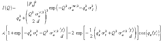
with, ![]()
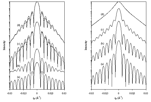
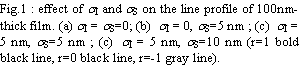
where su(c), sI, sS, and r are the rms lattice displacements, the rms interface roughness, the rms surface roughness and interface-surface roughness correlation coefficient (r=1 correlated, r=0 uncorrelated, r=-1 anti-correlated). The effects of these microstructural parameters (computed with the above equation) are shown in fig.1 and fig. 2. and will be further discussed at the conference together with the assumptions made.
[1] W. Friedrich, P. Knipping, M. Laue, Annalen der Physik 14, 971-990, 1913.
[2]R. L Snyder, J. Fiala, H. J. Bunge (Eds), Defect and microstructure analysis by diffraction, IUCr Monographs on crystallography 10 (Oxford University Press Inc, New-York) 1999.
[3] E. J. Mittemeijer, P. Scardi (Eds), Diffraction analysis of the microstructure of materials, Springer series in materials science (Springer-Verlag, Berlin Heidelberg) 2004.
[4] A. Authier, Dynamical theory of X-ray diffraction, IUCr monographs on crystallography 11. (Oxford University Press, New-York) 2001.
[5] P. F. Miceli, C. J. Palmstrom, K. W. Moyers, Appl. Phys. Lett. 61 17, 2060-2062, 1992.
[6] E. Zolotoyabko, J. Appl. Cryst. 31, 241-251, 1998.
[7] A. Boulle, R. Guinebretière, A. Dauger, J. Phys. IV France (2004) to be published.