Transrotational thin-film crystals
V. Yu. Kolosov
Physics Department, Ural Federal University, Lenin Av.51, Ekaterinburg
620000, Russia
kolosov@urfu.ru
The paper accumulates our novel studies and main former data on novel microstructure with unexpected, dislocation independent, regular internal bending of the crystal lattice planes [1]. Usually it is revealed in thin films or layers after amorphous – crystalline transitions. Such perfect crystals/grains with regularly curved lattice (built up by simultaneous translation and small regular rotation of the unit cell) demonstrate a new “transrotational” [2] type of solid state order realized in thin films. It is primarily dislocation independent and takes place round an axis (or 2 axes, Figure 1) lying in the film plane of the growing crystal. The maximal values correspond to essential lattice orientation gradients (up to 300 degrees per µm) resulting to several whole rotations for the crystal about 10 µm in length (in film plane).
Thin (10 - 100 nm) crystallized areas with we study vary from small crystals (0.1 - 100 microns), ribbons, whiskers or spherulites to large-scaled polycrystalline areas with a complex texture. They can be grown with the help of heat treatment (or aging) and local annealing by focused electron (or laser beam) in amorphous films of substances of different chemical nature including oxides, chalcogen/ides, some metals and alloys (with or without amorphous sublayers and overlayers) and are stable with years. The films were prepared by laser, e-beam and thermal evaporation mostly with thickness or/and composition gradients across TEM grids (to study these factors directly), solid state amorphization, pyrolysis. The main data have been obtained by TEM, primarily bend-contour method [3], in situ studies, and HREM with EDX, EELS, CBED used in due cases. Comparative TEM-AFM studies were performed for definite transrotational microcrystals in amorphous matrix.
Opposite to other unusual regular nano aggregations of atoms widely recognized by the community in recent 30 years (quasi-crystals, fullerenes and nanotubes and other nano derivatives) our less known “transrotational” crystals/structures are less confined in dimensions. Bent atom layers in fine areas can be described as similar to that of hypothetical 2.5D halves (180°) of endless (continuous in film plane) multiwall nano- tubes/onions/tori. The geometry and the magnitude of transrotation depends upon the substance, film preparation and crystallization conditions, orientation of the crystal nucleus, presence of the sublayers, composition and film thickness. In situ studies in particular include HREM of amorphous-crystalline interface propagation during crystal growth and multiple reversible local transformations "amorphous – transrotational crystalline” inside the fingers in Se-based vacuum deposits, Figure 4. Dynamic changes of TEM diffraction contrast (revealed by analysis of the video for the large Vg) fit the mechanism of transrotation formation based on the surface nucleation that we proposed earlier.
Most substantial are several examples of “transrotational single crystals” grown in the absence of grain boundaries and dislocations (See – Figure 2, Te and chalcogenide whiskers/nanobelts, e.g. CuTe, right on Figure 3) and also other perfect crystals with limited imperfection.
Atomistic mathematical model (based on conformal transformations) for the atom positions in "transrotational" single microcrystal and the probable physical reasons are discussed. Transrotational microstructure can be considered as an intermediate between amorphous and crystalline (likewise the structure of liquid crystals, intermediate between crystalline structure and liquid one). We reflect it as one of the reasons of easy phase changes in chalcogen-based films which tend to crystallize in such manner. Transrotational crystals during last years have been eventually recognized/studied in a large variety of thin film systems: Se-C, Se-Te, Sb2Se3, Sb2S3, Ge-Sb2Se3, Ge-Te, Tl-Se, Cu-Te, a‑Fe2O3, Cr2O3, Co-Pd, Re, W, carbides, amorphous metals, ferroelectrics, etc., including well-known chalcogenide compositions [4, 5] used for optical memory (CD-RW, DVD RW disks) and prospective for other memories.
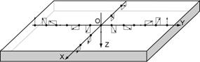 |
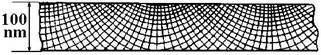
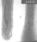
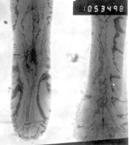
Figure 1. Regular changes of lattice orientation revealed by TEM in thin crystals with 2-axes lattice bending (left) and corresponding scheme of internal bending of lattice planes (right) shown in film cross section.
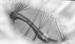
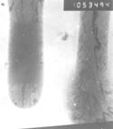
Figure 2. TEM image of transrotational Se single crystal (left) with one of the sequential SAED patterns (right) from the zone-axis pattern marked by selected area 1 µm aperture
|
|
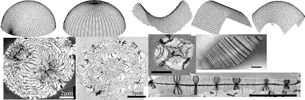
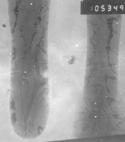
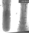
Figure 3 Schemes of transrotation geometry with the TEM images below: Se, Fe2O3, Ta2O5, C+Se+C, Cu-Te. Bar = 1 µm (where not specified)
|
|