Short and long range order analysis (Amorphous to Crystalline) using Electron Diffraction
P. P. Das, S. Nicolopoulos
NanoMEGAS SPRL,Blvd Edmond Machtens 79,B-1080, Brussels,
Belgium
partha@ecrystsolutions.com
Understanding and possible prediction of interesting properties of a material depends upon heavily on the precise knowledge of the atomic structure of the material. The structural ordering of the material can vary from very short range ordering/no ordering (amorphous materials) to longer range ordering (crystalline materials).Transmission electron microscopy (TEM) allows to study materials with varying degree of order using Electron Diffraction (ED) techniques. Here we present how ED can be used to study materials from ordered nanoparticles to amorphous.
Materials having long range order will show always Bragg diffraction peaks .To solve their crystal structure, 3D diffraction tomography data (coupled with beam precession) can be collected on a single crystal of suitable size (40 nm -200 nm) and rotating the crystal around an arbitrary axis . Such 3D precession diffraction tomography data [1] can be analysed using software that allows semi-automatic unit cell determination and measure reflection intensities. Extracted intensities can be used to reveal all atomic coordinates in the structure.
On the other hand, any type of structural disorder/ defects may results in ED diffuse scattering and in many cases even complete disappearance of Bragg reflections (case of amorphous materials). In such cases Pair Distribution Function (PDF) analysis [2] calculated from ED data can be used very successfully to study local structural environment and the degree of long/short range order of the material (amorphous or nanocrystalline). In our work here we present two examples : one case considering NaYF4 nanoparticles where PDF analysis shows clearly existence of long range order (nanoparticle case) and in another case we consider amorphous Opal mineral where using PDF analysis only short range order is visible (until 0.8 nm). In addition, ED related techniques like ASTAR (orientation imaging in TEM) allows to analyse at nm scale precise amorphous and crystalline areas, revealing the true order of complex materials [3].
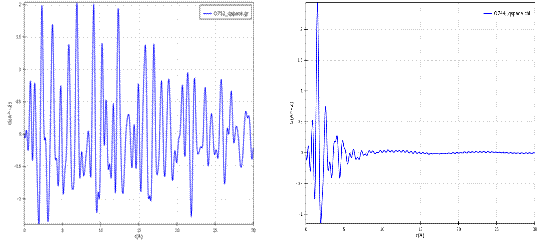
Figure 1. Pair Distribution Function for a Nanoparticle (long range order) (left image) and an amorphous opal (right image) mineral which shows only short range ordering < 0.8 nm
1. E. Mugnaiolo, T. Gorelik, U. Kolb, Ultramicroscopy, 109, (2009), 758.
2. G. R. Anstis, Z. Liu, M. Lake, Ultramicroscopy, 26, (1988), 65
3. E. F. Rauch, M. Veron, J. Portillo, D. Bultreys, Y. Maniette, S. Nicolopupos, Microsc. and Anal., 93, (2008), S5.
Author would like to Thank Dr. Mauro Gemmi (Center for Nanotechnology Innovation @NEST, Istituto Italiano di Tecnologia, Pisa, Italy) for the PDF data collection.